ACS8520 データシートの表示(PDF) - Semtech Corporation
部品番号
コンポーネント説明
メーカー
ACS8520 Datasheet PDF : 150 Pages
| |||
ACS8520 SETS
ADVANCED COMMUNICATIONS
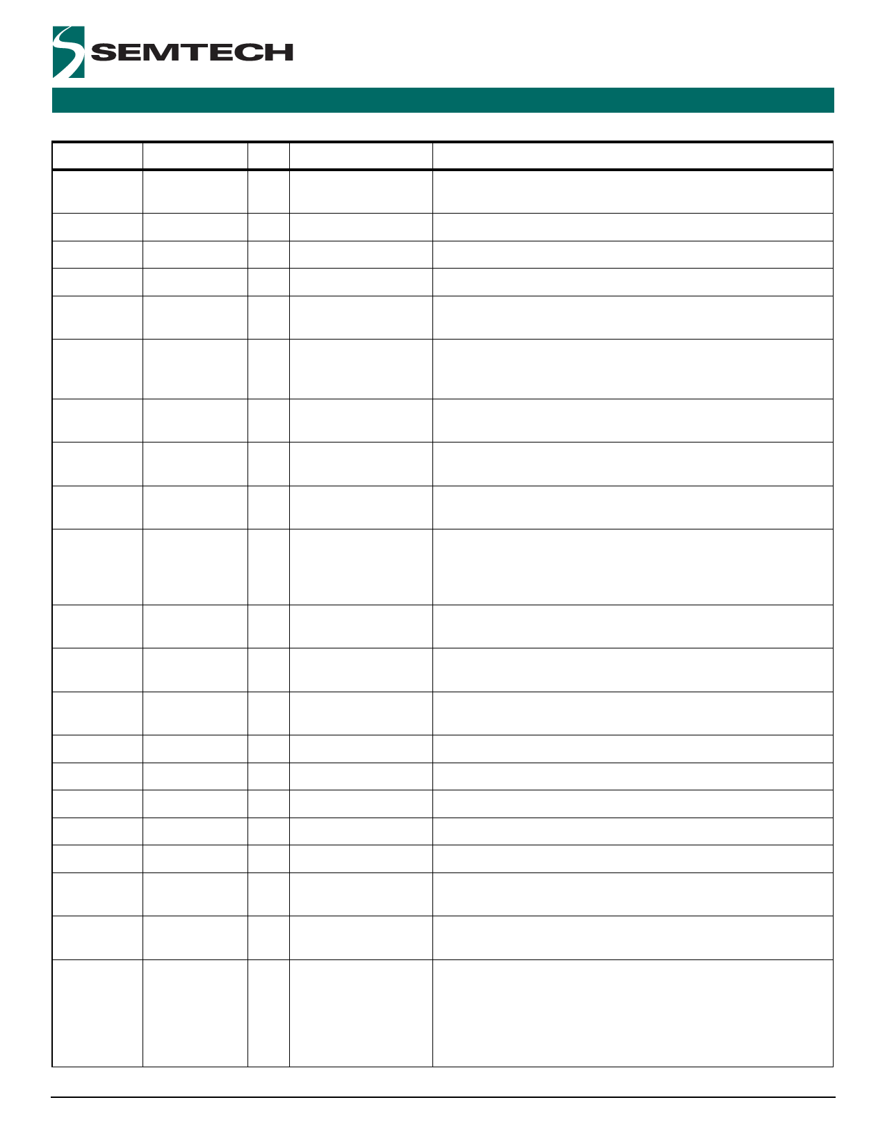
Table 3 Other Pins (cont...)
Pin Number
Symbol
I/O
Type
54
I11
I
TTLD
55
I12
I
56
I13
I
57
I14
I
58 - 60
UPSEL(2:0)
I
TTLD
TTLD
TTLD
TTLD
63 - 69
A(6:0)
I
TTLD
70
CSB
71
WRB
72
RDB
73
ALE
I
TTLU
I
TTLU
I
TTLU
I
TTLD
74
PORB
I
TTLU
75
RDY
O
TTL/CMOS
76 - 83
88
89
90
93
94
95
99
AD(7:0)
TO1
TO2
TO3
TO4
TO5
TO9
MSTSLVB
IO
TTLD
O
TTL/CMOS
O
TTL/CMOS
O
TTL/CMOS
O
TTL/CMOS
O
TTL/CMOS
O
TTL/CMOS
I
TTLU
100
SONSDHB
I
TTLD
FINAL
DATASHEET
Description
Input Reference 11: Programmable, default (Master mode)
1.544/2.048 MHz, default (Slave mode) 6.48 MHz.
Input Reference 12: Programmable, default 1.544/2.048 MHz.
Input Reference 13: Programmable, default 1.544/2.048 MHz.
Input Reference 14: Programmable, default 1.544/2.048 MHz.
Microprocessor Select: Configures the interface for a particular
microprocessor type at reset.
Microprocessor Interface Address: Address bus for the microprocessor
interface registers. A(0) is SDI in Serial mode - output in EPROM mode
only. A(1) is CLKE in serial mode.
Chip Select (Active Low): This pin is asserted Low by the microprocessor
to enable the microprocessor interface - output in EPROM mode only.
Write (Active Low): This pin is asserted Low by the microprocessor to
initiate a write cycle. In Motorola mode, WRB = 1 for Read.
Read (Active Low): This pin is asserted Low by the microprocessor to
initiate a read cycle.
Address Latch Enable: This pin becomes the address latch enable from
the microprocessor. When this pin transitions from High to Low, the
address bus inputs are latched into the internal registers. ALE = SCLK in
Serial mode.
Power-On Reset: Master reset. If PORB is forced Low, all internal states
are reset back to default values.
Ready/Data Acknowledge: This pin is asserted High to indicate the
device has completed a read or write operation.
Address/Data: Multiplexed data/address bus depending on the
microprocessor mode selection. AD(0) is SDO in Serial mode.
Output Reference 1: Programmable, default 6.48 MHz.
Output Reference 2: Programmable, default 38.88 MHz.
Output Reference 3: Programmable, default 19.44 MHz.
Output Reference 4: Programmable, default 38.88 MHz.
Output Reference 5: Programmable, default 77.76 MHz.
Output Reference 9: 1.544/2.048 MHz, as per ITU G.783[9] BITS
requirements.
Master/Slave Select: Sets the state of the Master/Slave selection
register, Reg. 34, Bit 1.
SONET or SDH Frequency Select: Sets the initial power-up state (or
state after a PORB) of the SONET/SDH frequency selection registers,
Reg. 34, Bit 2 and Reg. 38, Bit 5, Bit 6 and Reg. 64 Bit 4.When set Low,
SDH rates are selected (2.048 MHz etc.) and when set High, SONET
rates are selected (1.544 MHz etc.) The register states can be changed
after power-up by software.
Revision 3.02/October 2005 © Semtech Corp.
Page 7
www.semtech.com
Share Link: 