AD5533BBCZ-1 データシートの表示(PDF) - Analog Devices
部品番号
コンポーネント説明
メーカー
AD5533BBCZ-1 Datasheet PDF : 16 Pages
| |||
AD5533B
TIMING CHARACTERISTICS
PARALLEL INTERFACE
Parameter1, 2
Limit at TMIN, TMAX
(B Version)
Unit
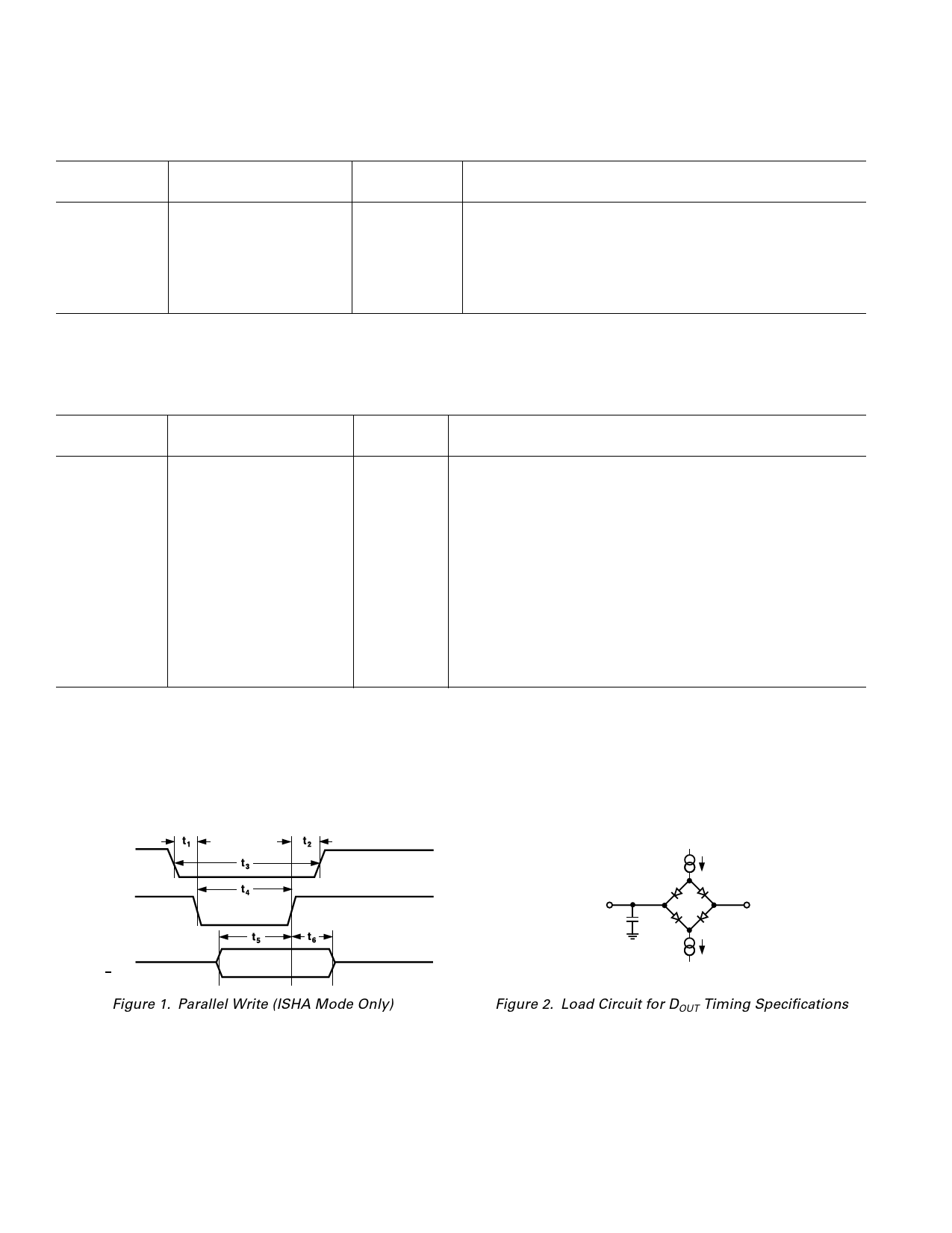
t1
0
t2
0
t3
50
t4
50
t5
20
t6
7
ns min
ns min
ns min
ns min
ns min
ns min
NOTES
1See Parallel Interface Timing Diagram.
2Guaranteed by design and characterization, not production tested.
Specifications subject to change without notice.
Conditions/Comments
CS to WR Setup Time
CS to WR Hold Time
CS Pulsewidth Low
WR Pulsewidth Low
A4–A0, CAL, OFFS_SEL to WR Setup Time
A4–A0, CAL, OFFS_SEL to WR Hold Time
SERIAL INTERFACE
Parameter1, 2
Limit at TMIN, TMAX
(B Version)
fCLKIN
20
t1
20
t2
20
t3
15
t4
50
t5
10
t6
5
t7
5
t83
20
t93
60
t10
400
t114
7
Unit
MHz max
ns min
ns min
ns min
ns min
ns min
ns min
ns min
ns max
ns max
ns min
ns min
NOTES
1See Serial Interface Timing Diagrams.
2Guaranteed by design and characterization, not production tested.
3These numbers are measured with the load circuit of Figure 2.
4SYNC should be taken low while SCLK is low for readback.
Specifications subject to change without notice.
Conditions/Comments
SCLK Frequency
SCLK High Pulsewidth
SCLK Low Pulsewidth
SYNC Falling Edge to SCLK Falling Edge Setup Time
SYNC Low Time
DIN Setup Time
DIN Hold Time
SYNC Falling Edge to SCLK Rising Edge Setup Time for Readback
SCLK Rising Edge to DOUT Valid
SCLK Falling Edge to DOUT High Impedance
10th SCLK Falling Edge to SYNC Falling Edge for Readback
SCLK Falling Edge to SYNC Falling Edge Setup Time for
Readback
PARALLEL INTERFACE TIMING DIAGRAM
CS
WR
A4–A0, CAL,
OFFS SEL
Figure 1. Parallel Write (ISHA Mode Only)
TO
OUTPUT
PIN
200A
IOL
CL
50pF
200A
IOH
1.6V
Figure 2. Load Circuit for DOUT Timing Specifications
–4–
REV. A
Share Link: 