AD5541BR(1999) データシートの表示(PDF) - Analog Devices
部品番号
コンポーネント説明
メーカー
AD5541BR Datasheet PDF : 12 Pages
| |||
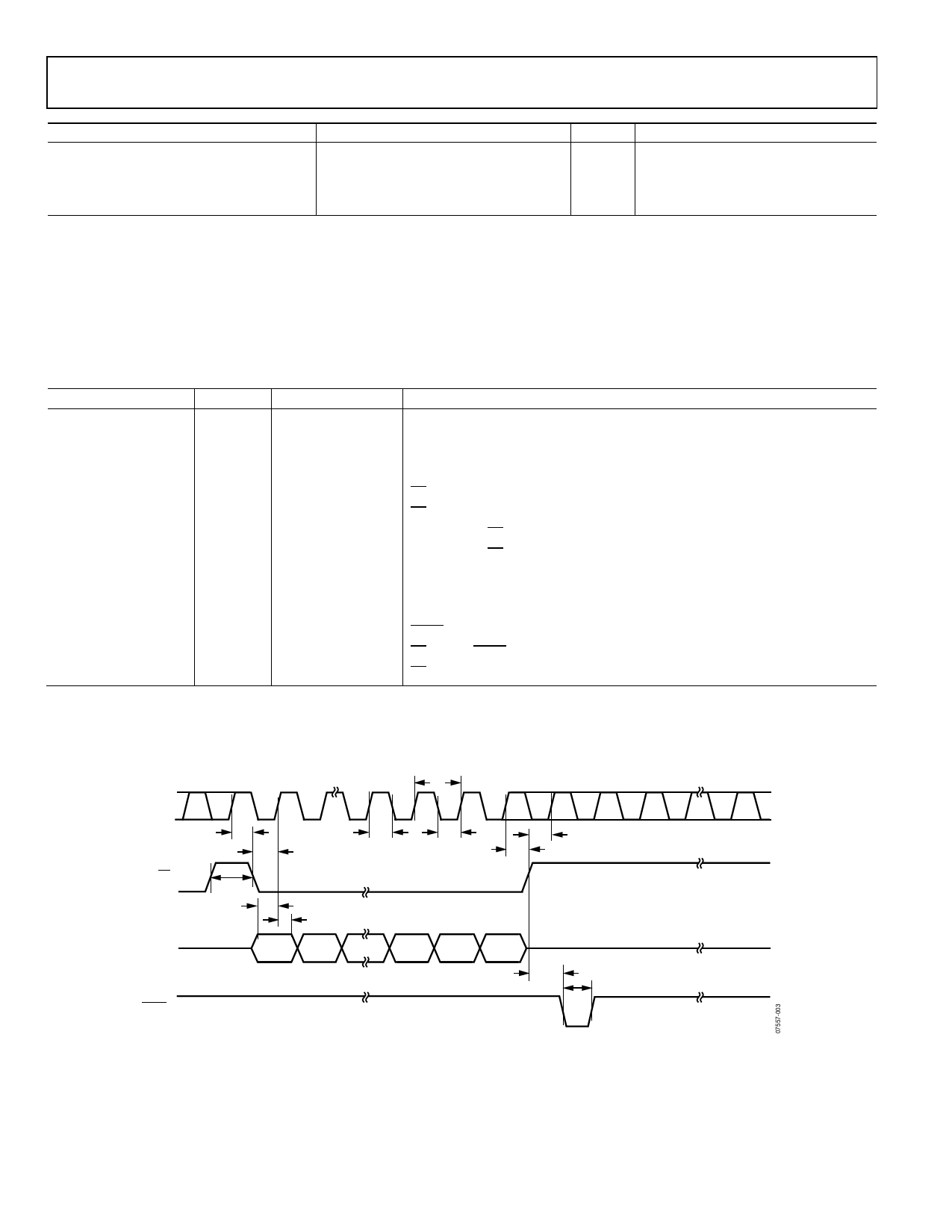
AD5541/AD5542
ABSOLUTE MAXIMUM RATINGS*
(TA = 25°C unless otherwise noted)
VDD to AGND . . . . . . . . . . . . . . . . . . . . . . . . . –0.3 V to +6 V
Digital Input Voltage to DGND . . . . . –0.3 V to VDD + 0.3 V
VOUT to AGND . . . . . . . . . . . . . . . . . . –0.3 V to VDD + 0.3 V
AGND, AGNDF, AGNDS to DGND . . . . . –0.3 V to +0.3 V
Input Current to Any Pin Except Supplies . . . . . . . . ± 10 mA
Operating Temperature Range
Industrial (A, B, C Versions) . . . . . . . . . . . –40°C to +85°C
Commercial (J, L Versions) . . . . . . . . . . . . . . . 0°C to 70°C
Storage Temperature Range . . . . . . . . . . . . –65°C to +150°C
Maximum Junction Temperature, (TJ max) . . . . . . . . . 150°C
Package Power Dissipation . . . . . . . . . . . . . (TJ max – TA)/θJA
Thermal Impedance θJA
SOIC (SO-8) . . . . . . . . . . . . . . . . . . . . . . . . . . 149.5°C/W
SOIC (R-14) . . . . . . . . . . . . . . . . . . . . . . . . . . 104.5°C/W
Lead Temperature, Soldering
Vapor Phase (60 sec) . . . . . . . . . . . . . . . . . . . . . . . . 215°C
Infrared (15 sec) . . . . . . . . . . . . . . . . . . . . . . . . . . . . 220°C
*Stresses above those listed under Absolute Maximum Ratings may cause perma-
nent damage to the device. This is a stress rating only; functional operation of the
device at these or any other conditions above those listed in the operational
sections of this specification is not implied. Exposure to absolute maximum rating
conditions for extended periods may affect device reliability.
ORDERING GUIDE
Model
INL
DNL
Temperature Range
AD5541CR
AD5541LR
AD5541BR
AD5541JR
AD5541AR
AD5542CR
AD5542LR
AD5542BR
AD5542JR
AD5542AR
± 1 LSB
± 1 LSB
± 2 LSB
± 2 LSB
± 4 LSB
± 1 LSB
± 1 LSB
± 2 LSB
± 2 LSB
± 4 LSB
± 1 LSB
± 1 LSB
± 1 LSB
± 1.5 LSB
± 1 LSB
± 1 LSB
± 1 LSB
± 1 LSB
± 1.5 LSB
± 1 LSB
–40°C to +85°C
0°C to 70°C
–40°C to +85°C
0°C to 70°C
–40°C to +85°C
–40°C to +85°C
0°C to 70°C
–40°C to +85°C
0°C to 70°C
–40°C to +85°C
Die Size = 80 × 139 = 11,120 sq mil; Number of Transistors = 1,230.
Package Description
8-Lead Small Outline IC
8-Lead Small Outline IC
8-Lead Small Outline IC
8-Lead Small Outline IC
8-Lead Small Outline IC
14-Lead Small Outline IC
14-Lead Small Outline IC
14-Lead Small Outline IC
14-Lead Small Outline IC
14-Lead Small Outline IC
Package Option
SO-8
SO-8
SO-8
SO-8
SO-8
R-14
R-14
R-14
R-14
R-14
CAUTION
ESD (electrostatic discharge) sensitive device. Electrostatic charges as high as 4000 V readily
accumulate on the human body and test equipment and can discharge without detection. Although
the AD5541/AD5542 features proprietary ESD protection circuitry, permanent damage may occur
on devices subjected to high-energy electrostatic discharges. Therefore, proper ESD precautions
are recommended to avoid performance degradation or loss of functionality.
WARNING!
ESD SENSITIVE DEVICE
–4–
REV. A
Share Link: 