AD5541LR データシートの表示(PDF) - Analog Devices
部品番号
コンポーネント説明
メーカー
AD5541LR Datasheet PDF : 20 Pages
| |||
AD5541/AD5542
Data Sheet
Parameter 1
POWER REQUIREMENTS
VDD
IDD
Power Dissipation
Min Typ
2.7
125
0.625
Max
5.5
150
0.825
1 Temperature ranges are as follows: A, B, C versions: −40°C to +85°C; J, L versions: 0°C to 70°C.
2 Reference input resistance is code-dependent, minimum at 0x8555.
3 Guaranteed by design, not subject to production test.
Unit
Test Conditions
Digital inputs at rails
V
μA
mW
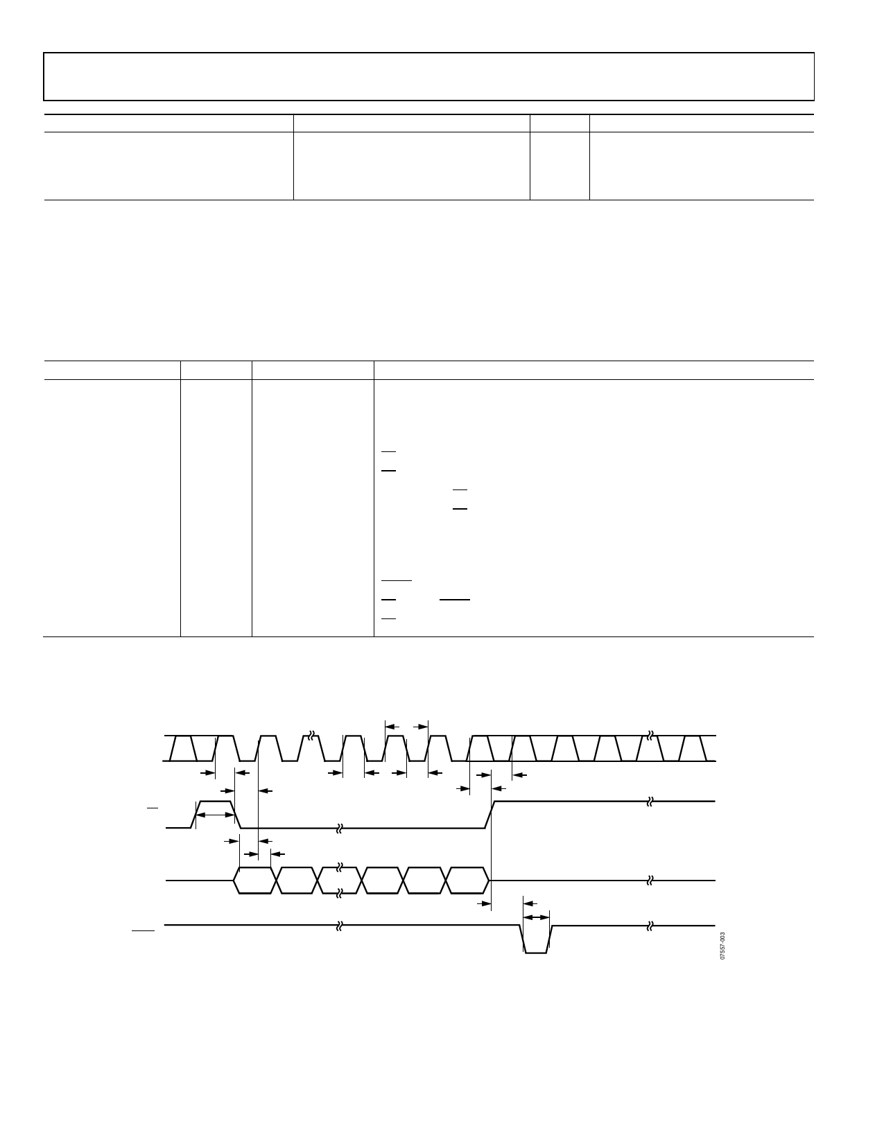
TIMING CHARACTERISTICS
VDD = 2.7 V to 5.5 V ±10%, VREF = 2.5 V, VINH = 3 V and 90% of VDD, VINL = 0 V and 10% of VDD, AGND = DGND = 0 V; −40°C < TA <
+85°C, unless otherwise noted.
Table 3.
Parameter1, 2
fSCLK
t1
t2
t3
t4
t5
t6
t7
t8
t9
t9
t10
t11
t12
Limit
25
40
20
20
10
15
30
20
15
4
7.5
30
30
30
Unit
MHz max
ns min
ns min
ns min
ns min
ns min
ns min
ns min
ns min
ns min
ns min
ns min
ns min
ns min
Description
SCLK cycle frequency
SCLK cycle time
SCLK high time
SCLK low time
CS low to SCLK high setup
CS high to SCLK high setup
SCLK high to CS low hold time
SCLK high to CS high hold time
Data setup time
Data hold time (VINH = 90% of VDD, VINL = 10% of VDD)
Data hold time (VINH = 3V, VINL = 0 V)
LDAC pulse width
CS high to LDAC low setup
CS high time between active periods
1 Guaranteed by design and characterization. Not production tested
2 All input signals are specified with tR = tF = 1 ns/V and timed from a voltage level of (VINL + VINH)/2.
t1
SCLK
t6
t4
CS
t12
t8
t5
t2
t3
t5
t7
DIN
DB15
t11
t10
LDAC*
*AD5542 ONLY. CAN BE TIED PERMANENTLY LOW IF REQUIRED.
Figure 3. Timing Diagram
Rev. F | Page 4 of 20
Share Link: 