EVAL-AD5750EBZ データシートの表示(PDF) - Analog Devices
部品番号
コンポーネント説明
メーカー
EVAL-AD5750EBZ Datasheet PDF : 36 Pages
| |||
Data Sheet
AD5750/AD5750-1/AD5750-2
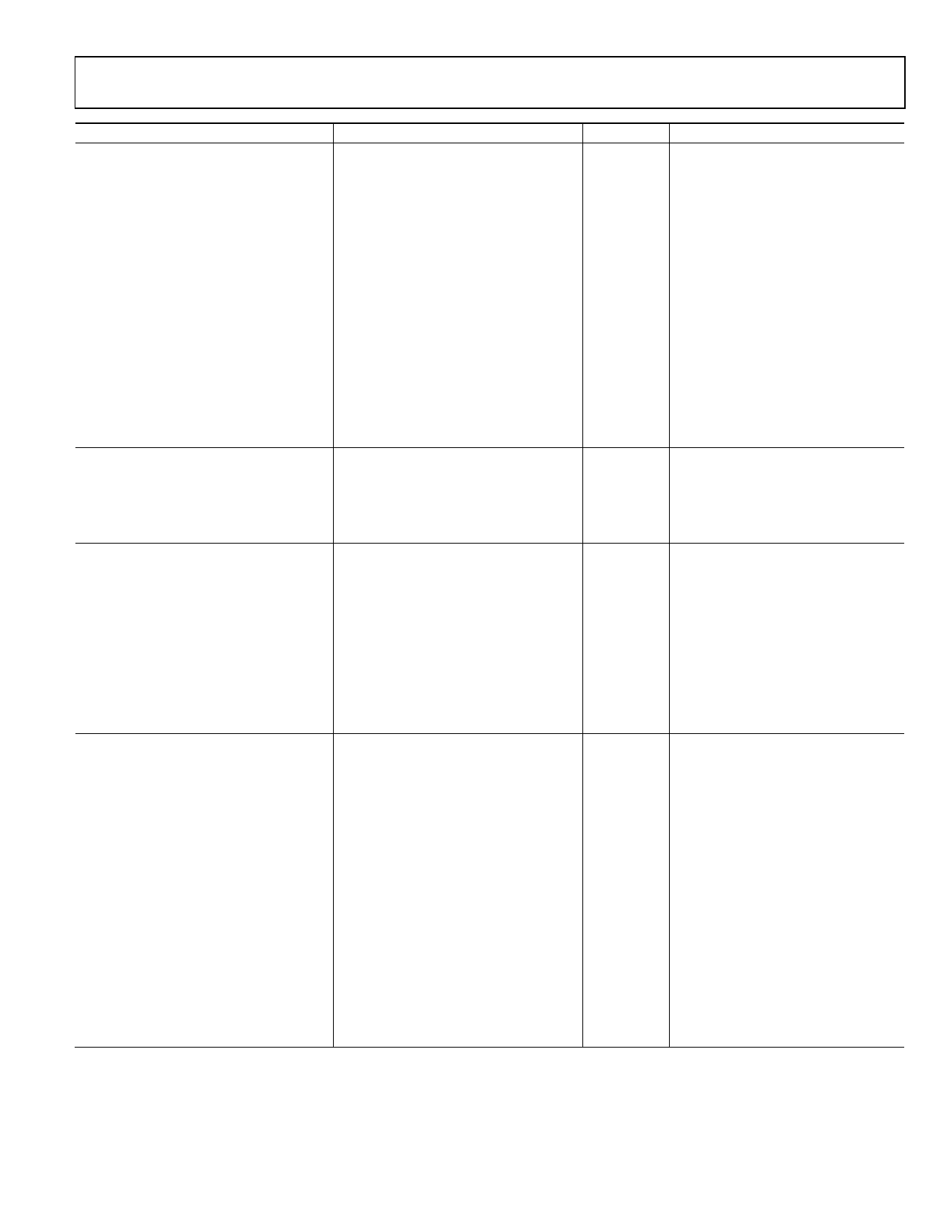
Parameter1
CURRENT OUTPUT CHARACTERISTICS3
Current Loop Compliance Voltage
Resistive Load
Inductive Load
Min
Typ
Max
Unit
0
AVDD − 2.75 V
See test conditions/comments column
See test conditions/comments column
Settling Time
4 mA to 20 mA, Full-Scale Step
4 mA to 20 mA, 120 µA Step
DC PSRR
Output Impedance
Leakage Current
VOUT/VSENSE− Error
8.5
1.2
130
−12
0.9994
1
+12
1.0006
µs
µs
µA/V
MΩ
nA
Gain
DIGITAL INPUT
Input High Voltage, VIH
2
V
Input Low Voltage, VIL
0.8
V
Input Current
−1
+1
µA
Pin Capacitance
5
pF
DIGITAL OUTPUTS3
FAULT, IFAULT, TEMP, VFAULT
Output Low Voltage, VOL
0.4
V
0.6
V
Output High Voltage, VOH
3.6
V
SDO
Output Low Voltage, VOL
0.5
0.5
V
Output High Voltage, VOH
DVCC − 0.5 DVCC − 0.5
V
High Impedance Output Capacitance
3
pF
High Impedance Leakage Current −1
+1
µA
POWER REQUIREMENTS
AVDD
12
24
V
AVSS
−12
−24
V
DVCC
Input Voltage
2.7
5.5
V
AIDD
4.4
5.6
mA
5.2
6.2
mA
5.2
6.2
mA
AISS
2.0
2.5
mA
DICC
Power Dissipation
2.0
3.5
mA
2.5
3
mA
2.5
3
mA
0.3
1
mA
108
mW
1 Temperature range: −40°C to +105°C; typical at +25°C.
2 Specification includes gain and offset errors over temperature and drift after 1000 hours, TA = 125°C.
3 Guaranteed by characterization, but not production tested.
Test Conditions/Comments
Chosen such that compliance is
not exceeded
Needs appropriate capacitor at
higher inductance values; see the
Driving Inductive Loads section
250 Ω load
250 Ω load
Output disabled; leakage to ground
Error in VOUT voltage due to changes
in VSENSE−; specified as gain, for
example, if VSENSE− moves by 1 V,
VOUT moves by 0.9994 V
JEDEC compliant
Per pin
Per pin
10 kΩ pull-up resistor to DVCC
At 2.5 mA
10 kΩ pull-up resistor to DVCC
Sinking 200 µA
Sourcing 200 µA
±10%
±10%
Output unloaded, output disabled,
R3, R2, R1, R0 = 0, 1, 0, 1; RSET = 0
Current output enabled
Voltage output enabled
Output unloaded, output disabled,
R3, R2, R1, R0 = 0, 1, 0, 1; RSET = 0,
AD5750 and AD5750-1
AD5750-2
Current output enabled
Voltage output enabled
VIH = DVCC, VIL = GND
AVDD/AVSS = ±24 V, outputs unloaded
Rev. D | Page 7 of 36
Share Link: 