EVAL-AD5765EBZ гГЗгГЉгВњгВЈгГЉгГИгБЃи°®з§ЇпЉИPDFпЉЙ - Analog Devices
йГ®еУБзХ™еПЈ
гВ≥гГ≥гГЭгГЉгГНгГ≥гГИи™ђжШО
гГ°гГЉгВЂгГЉ
EVAL-AD5765EBZ Datasheet PDF : 28 Pages
| |||
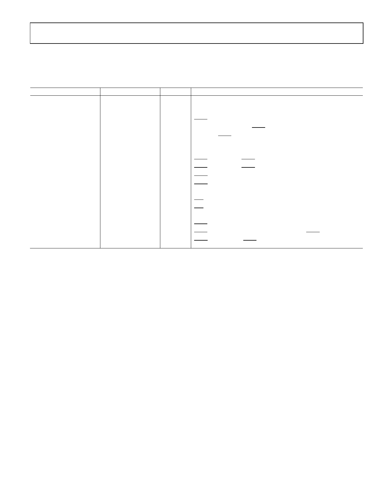
Data Sheet
AD5765
TIMING CHARACTERISTICS
AVDD = 4.75 V to 5.25 V, AVSS = вИТ4.75 V to вИТ5.25 V, AGNDx = DGND = REFGND = PGND = 0 V, REFAB = REFCD = 2.048 V,
DVCC = 2.7 V to 5.25 V, RLOAD = 5 kвД¶, CLOAD = 200 pF. All specifications TMIN to TMAX, unless otherwise noted.
Table 4.
Parameter1, 2, 3
t1
t2
t3
t4
t54
t6
t7
t8
t9
t10
t11
t12
t13
t14
t155, 6
t16
t17
t18
Limit at TMIN, TMAX
33
13
13
13
13
90
2
5
1.7
480
10
500
10
10
2
25
13
2
170
Unit
ns min
ns min
ns min
ns min
ns min
ns min
ns min
ns min
µs min
ns min
ns min
ns max
µs max
ns min
µs max
ns max
ns min
µs max
ns min
Description
SCLK cycle time
SCLK high time
SCLK low time
SYNC falling edge to SCLK falling edge setup time
24th SCLK falling edge to SYNC rising edge
Minimum SYNC high time
Data setup time
Data hold time
SYNC rising edge to LDAC falling edge when all DACs are updated
SYNC rising edge to LDAC falling edge when a single DAC is updated
LDAC pulse width low
LDAC falling edge to DAC output response time
DAC output settling time
CLR pulse width low
CLR pulse activation time
SCLK rising edge to SDO valid
SYNC rising edge to SCLK falling edge
SYNC rising edge to DAC output response time (LDAC = 0)
LDAC falling edge to SYNC rising edge
1 Guaranteed by design and characterization; not production tested.
2 All input signals are specified with tR = tF = 5 ns (10% to 90% of DVCC) and timed from a voltage level of 1.2 V.
3 See Figure 2, Figure 3, and Figure 4.
4 Standalone mode only.
5 Measured with the load circuit of Figure 5.
6 Daisy-chain mode only.
Rev. C | Page 7 of 28
Share Link: 