EVAL-AD5780SDZ гғҮгғјгӮҝгӮ·гғјгғҲгҒ®иЎЁзӨәпјҲPDFпјү - Analog Devices
йғЁе“Ғз•ӘеҸ·
гӮігғігғқгғјгғҚгғігғҲиӘ¬жҳҺ
гғЎгғјгӮ«гғј
EVAL-AD5780SDZ Datasheet PDF : 27 Pages
| |||
Data Sheet
System Ready, 18-Bit Вұ1 LSB INL,
Voltage Output DAC
AD5780
FEATURES
True 18-bit voltage output DAC, Вұ1 LSB INL
8 nV/вҲҡHz output noise spectral density
0.025 LSB long-term linearity error stability
Вұ0.018 ppm/В°C gain error temperature coefficient
2.5 Вөs output voltage settling time
3.5 nV-sec midscale glitch impulse
Integrated precision reference buffers
Operating temperature range: вҲ’40В°C to +125В°C
4 mm Г— 5 mm LFCSP package
Wide power supply range of up to Вұ16.5 V
35 MHz Schmitt triggered digital interface
1.8 V-compatible digital interface
APPLICATIONS
Medical instrumentation
Test and measurement
Industrial control
Scientific and aerospace instrumentation
Data acquisition systems
Digital gain and offset adjustment
Power supply control
GENERAL DESCRIPTION
The AD57801 is a true 18-bit, unbuffered voltage output digital-
to-analog converter (DAC) that operates from a bipolar supply
of up to 33 V. The AD5780 accepts a positive reference input
range of 5 V to VDD вҲ’ 2.5 V and a negative reference input range
of VSS + 2.5 V to 0 V. Both reference inputs are buffered on chip
and external buffers are not required. The AD5780 offers a
relative accuracy specification of Вұ1 LSB maximum range, and
operation is guaranteed monotonic with a Вұ1 LSB differential
nonlinearity (DNL) maximum range specification.
The part uses a versatile 3-wire serial interface that operates at
clock rates of up to 35 MHz and is compatible with standard
serial peripheral interface (SPI), QSPIв„ў, MICROWIREв„ў, and
DSP interface standards. The part incorporates a power-on
reset circuit that ensures that the DAC output powers up to 0 V
in a known output impedance state and remains in this state
until a valid write to the device takes place. The part provides
an output clamp feature that places the output in a defined load
state.
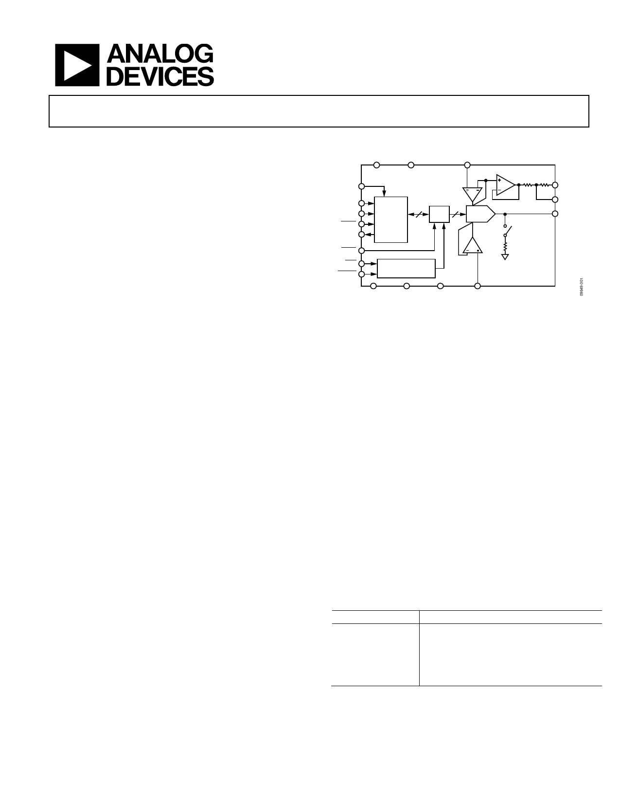
IOVCC
SDIN
SCLK
SYNC
SDO
LDAC
CLR
RESET
FUNCTIONAL BLOCK DIAGRAM
VCC
VDD
VREFP
AD5780
INPUT
SHIFT
18
REGISTER
AND
CONTROL
LOGIC
DAC 18
REG
18-BIT
DAC
R1 RFB
6.8kв„Ұ 6.8kв„Ұ
A1
RFB
INV
VOUT
6kв„Ұ
POWER-ON RESET
AND CLEAR LOGIC
DGND
VSS
AGND
VREFN
Figure 1.
PRODUCT HIGHLIGHTS
1. True 18-bit accuracy.
2. Wide power supply range of up to Вұ16.5 V.
3. вҲ’40В°C to +125В°C operating temperature range.
4. Low 8 nV/вҲҡHz noise.
5. Low Вұ0.018 ppm/В°C gain error temperature coefficient.
COMPANION PRODUCTS
Output Amplifier Buffer: AD8675, ADA4898-1, ADA4004-1
External Reference: ADR445, ADR4550
DC-to-DC Design Tool: ADIsimPowerв„ў
Additional companion products on the AD5780 product page.
Table 1. Related Devices
Part No.
Description
AD5790
20-bit, 2 LSB accurate DAC
AD5791
20-bit, 1 ppm accurate DAC
AD5781
18-bit, 0.5 LSB accurate DAC
AD5541A/AD5542A 16-bit, 1 LSB accurate 5 V DAC
AD5760
16-bit, 0.5 LSB accurate DAC
1 Protected by U.S. Patent No. 7,884,747 and 8,089,380.
Rev. F
Document Feedback
Information furnished by Analog Devices is believed to be accurate and reliable. However, no
responsibility is assumed by Analog Devices for its use, nor for any infringements of patents or other
rights of third parties that may result from its use. Specifications subject to change without notice. No
license is granted by implication or otherwise under any patent or patent rights of Analog Devices.
Trademarks and registered trademarks are the property of their respective owners.
One Technology Way, P.O. Box 9106, Norwood, MA 02062-9106, U.S.A.
Tel: 781.329.4700 В©2011вҖ“2018 Analog Devices, Inc. All rights reserved.
Technical Support
www.analog.com
Share Link: 