AD5930 データシートの表示(PDF) - Analog Devices
部品番号
コンポーネント説明
メーカー
AD5930 Datasheet PDF : 28 Pages
| |||
Data Sheet
AD5930
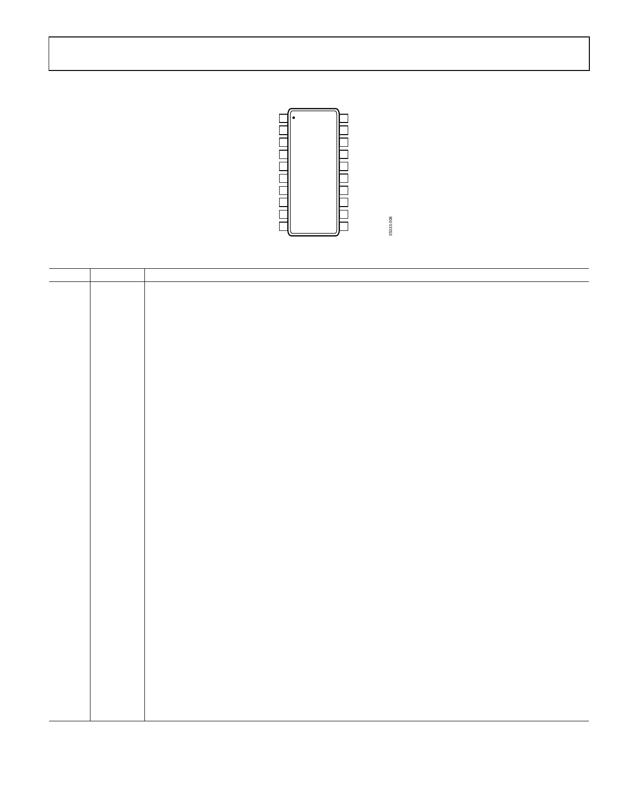
PIN CONFIGURATION AND FUNCTION DESCRIPTIONS
FSADJUST 1
20 IOUTB
REF 2
19 IOUT
COMP 3
AVDD 4
DVDD 5
AD5930
TOP VIEW
(Not to Scale)
18 AGND
17 STANDBY
16 FSYNC
CAP/2.5V 6
15 SCLK
DGND 7
14 SDATA
MCLK 8
13 CTRL
SYNCOUT 9
12 INTERRUPT
MSBOUT 10
11 DGND O/P
Figure 8. Pin Configuration
Table 4. Pin Function Descriptions
Pin No. Mnemonic Description
1
FSADJUST Full-Scale Adjust Control. A resistor (RSET) must be connected externally between this pin and AGND.
This determines the magnitude of the full-scale DAC current. The relationship between RSET and the
full-scale current is:
IOUTFULL-SCALE = 18 × VREFOUT/RSET
where VREFOUT = 1.20 V nominal and RSET = 6.8 kΩ typical.
2
REF
Voltage Reference. This pin can be an input or an output. The AD5930 has an internal 1.18 V reference, which
is made available at this pin. Alternatively, this reference can be overdriven by an external reference, with a
voltage range as given in the Specifications section. A 10 nF decoupling capacitor should be connected
between REF and AGND.
3
COMP
DAC Bias Pin. This pin is used for decoupling the DAC bias voltage to AVDD.
4
AVDD
Positive Power Supply for the Analog Section. AVDD can have a value from +2.3 V to +5.5 V. A 0.1 µF decoupling
capacitor should be connected between AVDD and AGND.
5
DVDD
Positive Power Supply for the Digital Section. DVDD can have a value from +2.3 V to +5.5 V. A 0.1 µF decoupling
capacitor should be connected between DVDD and DGND.
6
CAP/2.5V Digital Circuitry. Operates from a 2.5 V power supply. This 2.5 V is generated from DVDD using an on-board
regulator. The regulator requires a decoupling capacitor of typically 100 nF, which is connected from CAP/2.5V
to DGND. If DVDD is equal to or less than 2.7 V, CAP/2.5V can be shorted to DVDD.
7
DGND
Ground for all Digital Circuitry. This excludes digital output buffers.
8
MCLK
Digital Clock Input. DDS output frequencies are expressed as a binary fraction of the frequency of MCLK.
The output frequency accuracy and phase noise are determined by this clock.
9
SYNCOUT Digital Output for Sweep Status Information. User selectable for end of sweep (EOS) or frequency increments
through the control register (SYNCOP bit). This pin must be enabled by setting Control Register Bit SYNCOPEN to 1.
10
MSBOUT Digital Output. The inverted MSB of the DAC data is available at this pin. This output pin must be enabled by
setting bit MSBOUTEN in the control register to 1.
11
DGND O/P Separate DGND Connection for Digital Output Buffers. Connect to DGND.
12
INTERRUPT Digital Input. This pins acts as an interrupt during a frequency sweep. A low to high transition is sampled by the
internal MCLK, which resets internal state machines. This results in the DAC output going to midscale.
13
CTRL
Digital Input. Triple function pin for initialization, start, and external frequency increments. A low-to-high transition,
sampled by the internal MCLK, is used to initialize and start internal state machines, which then execute the pre-
programmed frequency sweep sequence. When in auto-increment mode, a single pulse executes the entire sweep
sequence. When in external increment mode, each frequency increment is triggered by a pulse.
14
SDATA
Serial Data Input. The 16-bit serial data-word is applied to this input with the register address first followed by the
MSB to LSB of the data.
15
SCLK
Serial Clock Input. Data is clocked into the AD5930 on each falling SCLK edge.
16
FSYNC
Active Low Control Input. This is the frame synchronization signal for the serial data. When FSYNC is taken low,
the internal logic is informed that a new word is being loaded into the device.
17
STANDBY Active High Digital Input. When this pin is high, the internal MCLK is disabled, and the reference DAC and regulator
are powered down. For optimum power saving, it is recommended to reset the AD5930 before putting it into
standby, as this results in a shutdown current of typically 20 µA.
Rev. D | Page 9 of 28
Share Link: 