LA4590W データシートの表示(PDF) - SANYO -> Panasonic
部品番号
コンポーネント説明
メーカー
LA4590W Datasheet PDF : 19 Pages
| |||
Continued from preceding page.
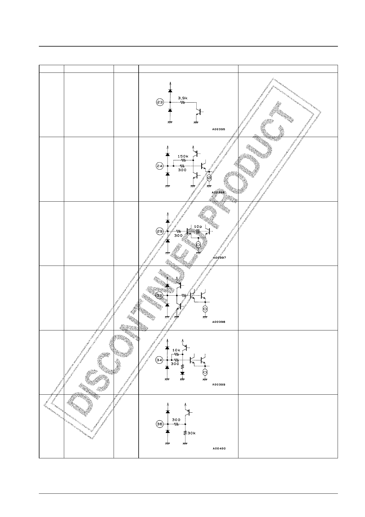
Pin No.
Symbol
VDC (V)
23
METAL1
0
26
METAL2
LA4590W
Equivalent circuit
Unit (resistance: Ω, capacitance: F)
Pin function
• Connected to ground by a 3.9 kΩ resistor when
metal is selected (pin 40 is floating).
24
AMS IN1
0.75
25
AMS IN2
29
PRE REV IN1
30
PRE REV IN2
0.75
31
PRE FWD IN2
32
PRE FWD IN1
33
VREF
0.75
34
REF
0.75
• AMS inverting input pins
• External input resistors must be connected to
these pins.
• Pins 29 and 30 are on in reverse mode (when
pin 39 is grounded).
• Pins 31 and 32 are on in forward mode (when
pin 39 is floating).
• When a particular head is not used, 2.2 kΩ bias
resistors must be inserted between the
corresponding pins and Vref (pin 33).
• Buzz suppression capacitors are built-in.
• VREF amplifier output pin. A built-in output
resistor (ro, about 10 Ω) makes this a low
impedance output.
• The current (inflow and outflow) capacity of this
pin is 200 µA, maximum.
• VREF amplifier reference
36
AMS OUT
• Outputs a pulse waveform that depends on the
AMS IN (pins 24 and 25) input levels.
Continued on next page.
No. 4468-7/19
Share Link: 