EVAL-CEDZ データシートの表示(PDF) - Analog Devices
部品番号
コンポーネント説明
メーカー
EVAL-CEDZ Datasheet PDF : 32 Pages
| |||
AD7264
PIN CONFIGURATION AND FUNCTION DESCRIPTIONS
48 47 46 45 44 43 42 41 40 39 38 37
CA_CBVCC 1
AVCC 2
VA– 3
VA+ 4
AGND 5
AGND 6
AVCC 7
AGND 8
VB+ 9
VB– 10
AVCC 11
CC_CDVCC 12
PIN 1
INDICATOR
AD7264
TOP VIEW
(Not to Scale)
36 CAL
35 CS
34 SCLK
33 AVCC
32 DOUTA
31 DOUTB
30 COUTA
29 COUTB
28 DGND
27 VDRIVE
26 COUTC
25 COUTD
13 14 15 16 17 18 19 20 21 22 23 24
CA_CBVCC 1
AVCC 2
VA– 3
VA+ 4
AGND 5
AGND 6
AVCC 7
AGND 8
VB+ 9
VB– 10
AVCC 11
CC_CDVCC 12
PIN 1
INDICATOR
AD7264
TOP VIEW
(Not to Scale)
36 CAL
35 CS
34 SCLK
33 AVCC
32 DOUTA
31 DOUTB
30 COUTA
29 COUTB
28 DGND
27 VDRIVE
26 COUTC
25 COUTD
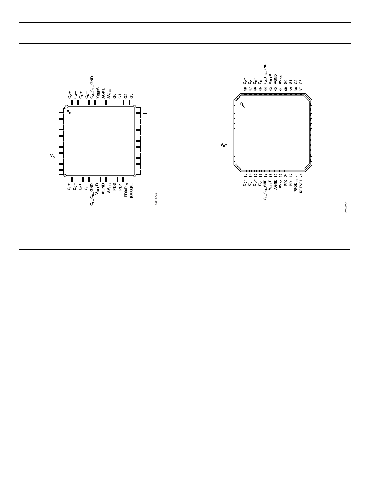
Figure 3. 48-Lead LQFP Pin Configuration
NOTES
1. THE EXPOSED METAL PADDLE ON THE BOTTOM OF THE LFCSP PACKAGE MUST
BE SOLDERED TO PCB GROUND FOR PROPER HEAT DISSIPATION AND ALSO FOR
NOISE AND MECHANICAL STRENGTH BENEFITS.
Figure 4. 48-Lead LFCSP Pin Configuration
Table 4. Pin Function Descriptions
Pin No.
Mnemonic
2, 7, 11, 20, 33, 41 AVCC
1
CA_CBVCC
12
CC_CDVCC
4, 3
9, 10
43, 18
VA+, VA−
VB+, VB−
VREFA, VREFB
34
SCLK
35
CS
36
CAL
21
PD2
22
PD1
23
PD0/DIN
Description
Analog Supply Voltage, 4.75 V to 5.25 V. This is the supply voltage for the analog circuitry on the
AD7264. All AVCC pins can be tied together. This supply should be decoupled to AGND with a 100 nF
ceramic capacitor per supply and a 10 μF tantalum capacitor.
Comparator Supply Voltage, 2.7 V to 5.25 V. This is the supply voltage for Comparator A and
Comparator B. This supply should be decoupled to CA_CB_GND. AVCC, CC_CDVCC, and CA_CBVCC can be
tied together.
Comparator Supply Voltage, 2.7 V to 5.25 V. This is the supply voltage for Comparator C and
Comparator D. This supply should be decoupled to CC_CD_GND. AVCC, CC_CDVCC, and CA_CBVCC can be
tied together.
Analog Inputs of ADC A. True differential input pair.
Analog Inputs of ADC B. True differential input pair.
Reference Input/Output. Decoupling capacitors are connected to these pins to decouple the
internal reference buffer for each respective ADC. Typically, 1 μF capacitors are required to decouple
the reference. Provided the output is buffered, the on-chip reference can be taken from these pins
and applied externally to the rest of a system.
Serial Clock. Logic input. A serial clock input provides the SCLK for accessing the data from the
AD7264. This clock is also used as the clock source for the conversion process. A minimum of
33 clocks are required to perform the conversion and access the 14-bit result.
Chip Select. Active low logic input. This input initiates conversions on the AD7264.
Logic Input. Initiates an internal offset calibration.
Logic Input. Places the AD7264 in the selected shutdown mode in conjunction with the PD1 and
PD0 pins. See Table 7.
Logic Input. Places the AD7264 in the selected shutdown mode in conjunction with the PD2 and
PD0 pins. See Table 7.
Logic Input/Data Input. Places the AD7264 in the selected shutdown mode in conjunction with the
PD2 and PD1 pins. See Table 7. If all gain selection pins, G0 to G3, are tied low, this pin acts as the
data input pin and all programming is via the control register (see Table 8). Data to be written to the
AD7264 control register is provided on this input and is clocked into the register on the falling edge
of SCLK.
Rev. A | Page 8 of 32
Share Link: 