AD7495ARM-REEL7 データシートの表示(PDF) - Analog Devices
部品番号
コンポーネント説明
メーカー
AD7495ARM-REEL7 Datasheet PDF : 24 Pages
| |||
AD7475/AD7495
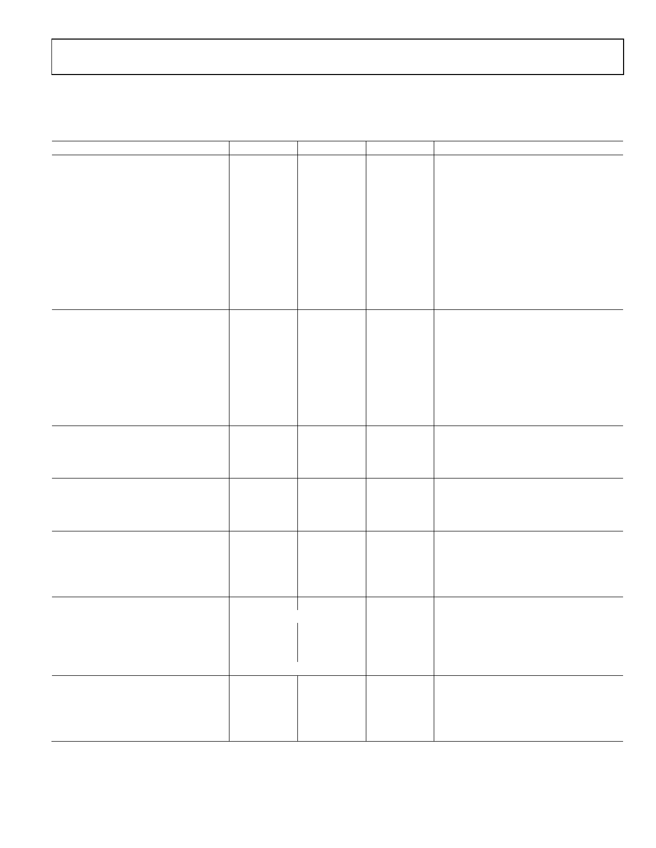
AD7495 SPECIFICATIONS
VDD = 2.7 V to 5.25 V, VDRIVE = 2.7 V to 5.25 V, fSCLK = 20 MHz, TA = TMIN to TMAX, unless otherwise noted.
Table 2.
Parameter
DYNAMIC PERFORMANCE
Signal-to-Noise and Distortion (SINAD)
Total Harmonic Distortion (THD)
Peak Harmonic or Spurious Noise
(SFDR)
Intermodulation Distortion (IMD)
Second-Order Terms
Third-Order Terms
Aperture Delay
Aperture Jitter
Full Power Bandwidth
Full Power Bandwidth
DC ACCURACY
Resolution
Integral Nonlinearity
Differential Nonlinearity
A Version1
68
−75
−76
−78
−78
10
50
8.3
1.3
12
±1.5
±0.5
+1.5/−0.9
B Version1
68
−75
−76
−78
−78
10
50
8.3
1.3
12
±1
±0.5
+1.5/−0.9
Unit
dB min
dB max
dB max
dB typ
dB typ
ns typ
ps typ
MHz typ
MHz typ
Bits
LSB max
LSB typ
LSB max
Offset Error
Gain Error
ANALOG INPUT
Input Voltage Ranges
DC Leakage Current
Input Capacitance
REFERENCE OUTPUT
REF OUT Output Voltage
REF OUT Impedance
REF OUT Temperature Coefficient
LOGIC INPUTS
Input High Voltage, VINH
Input Low Voltage, VINL
Input Current, IIN
Input Capacitance, CIN2
LOGIC OUTPUTS
Output High Voltage, VOH
Output Low Voltage, VOL
Floating-State Leakage Current
Floating-State Output Capacitance
Output Coding
CONVERSION RATE
Conversion Time
Track-and-Hold Acquisition Time
Throughput Rate
±0.6
±0.6
LSB typ
±8
±8
LSB max
±7
±7
LSB max
0 to 2.5
±1
20
0 to 2.5
±1
20
V
μA max
pF typ
2.4625/2.5375 2.4625/2.5375 V min/max
10
10
Ω typ
50
50
ppm/°C typ
VDRIVE − 1
0.4
±1
10
VDRIVE − 1
0.4
±1
10
V min
V max
μA max
pF max
VDRIVE − 0.2
0.4
0.4
±10
±10
10
10
Straight (Natural) Binary
V min
V max
μA max
pF max
800
800
ns max
300
300
ns max
325
325
ns max
1
1
MSPS max
Test Conditions/Comments
fIN = 300 kHz sine wave, fSAMPLE = 1 MSPS
fIN = 300 kHz sine wave, fSAMPLE = 1 MSPS
fIN = 300 kHz sine wave, fSAMPLE = 1 MSPS
@ 3 dB
@ 0.1 dB
@ 5 V (typ @ 3 V)
@ 25°C
@ 5 V guaranteed no missed codes to
12 bits (typ @ 3 V)
@ 25°C
Typically ±2.5 LSB
Typically ±2.5 LSB
Typically 10 nA, VIN = 0 V or VDRIVE
ISOURCE = 200 μA; VDD = 2.7 V to 5.25 V
ISINK = 200 μA
16 SCLK cycles with SCLK at 20 MHz
Sine wave input
Full-scale step input
See the Serial Interface section
Rev. B | Page 5 of 24
Share Link: 