AD7492ARUZ-5 データシートの表示(PDF) - Analog Devices
部品番号
コンポーネント説明
メーカー
AD7492ARUZ-5 Datasheet PDF : 24 Pages
| |||
AD7492
TIMING SPECIFICATIONS
VDD = 2.7 V to 5.25 V, TA = TMIN to TMAX, unless otherwise noted.1
Table 3.
Parameter
tCONVERT
tWAKEUP
t1
t2
Limit at TMIN, TMAX
AD7492/AD7492-4 AD7492-52
880
680
203
203
500
500
10
10
10
10
40
N/A
Unit
ns max
μs max
μs max
ns min
ns max
ns max
t3
0
t4 4
0
t5
20
t64
15
t7 5
8
t8
0
t9
120
t10
100
0
ns max
0
ns max
20
ns min
15
ns min
8
ns max
0
ns max
120
ns min
100
ns min
Description
Partial Sleep Wake-Up Time
Full Sleep Wake-Up Time
CONVST Pulse Width
CONVST to BUSY Delay, VDD = 5 V
CONVST to BUSY Delay, VDD = 3 V
BUSY to CS Setup Time
CS to RD Setup Time
RD Pulse Width
Data Access Time after Falling Edge of RD
Bus Relinquish Time after Rising Edge of RD
CS to RD Hold Time
Acquisition Time
Quiet Time
1 Sample tested @ 25°C to ensure compliance. All input signals are specified with tR = tF = 5 ns (10% to 90% of VDD) and timed from a voltage level of 1.6 V (see Figure 2).
2 The AD7492-5 is specified with VDD = 4.75 V to 5.25 V.
3 This is the time needed for the part to settle within 0.5 LSB of its stable value. Conversion can be initiated earlier than 20 μs, but there is no guarantee that the part
samples within 0.5 LSB of the true analog input value. Therefore, the user should not start conversion until after the specified time.
4 Measured with the load circuit of Figure 2 and defined as the time required for the output to cross 0.8 V or 2.0 V
5 t7 is derived from the measured time taken by the data outputs to change 0.5 V when loaded with the circuit of Figure 2. The measured number is then extrapolated
back to remove the effects of charging or discharging the 50 pF capacitor. This means that the time, t7, quoted in the timing characteristics is the true bus relinquish
time of the part and is independent of the bus loading.
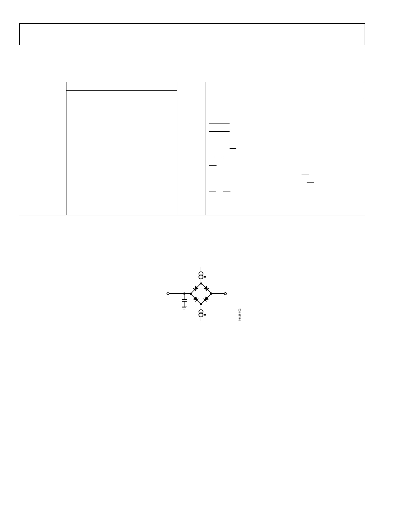
200µA
IOL
TO OUTPUT
PIN
CL
50pF
1.6V
200µA
IOH
Figure 2. Load Circuit for Digital Output Timing Specifications
Rev. A | Page 6 of 24
Share Link: 