AD7477AAKS-500RL7 データシートの表示(PDF) - Analog Devices
部品番号
コンポーネント説明
メーカー
AD7477AAKS-500RL7 Datasheet PDF : 24 Pages
| |||
AD7476A/AD7477A/AD7478A
TIMING SPECIFICATIONS1
(VDD = 2.35 V to 5.25 V; TA = TMIN to TMAX, unless otherwise noted.)
Parameter
Limit at TMIN, TMAX
AD7476A/AD7477A/AD7478A
Unit
Description
fSCLK 2
tCONVERT
tQUIET
t1
t2
t34
t44
t5
t6
t75
t86
tPOWER-UP8
10
20
20
16 ϫ tSCLK
14 ϫ tSCLK
12 ϫ tSCLK
50
10
10
22
40
0.4 tSCLK
0.4 tSCLK
10
9.5
7
36
See Note 7
1
kHz min3
kHz min3
MHz max
ns min
ns min
ns min
ns max
ns max
ns min
ns min
ns min
ns min
ns min
ns max
ns min
µs max
A, B Grades
Y Grade
AD7476A
AD7477A
AD7478A
Minimum Quiet Time Required between Bus Relinquish
and Start of Next Conversion
Minimum CS Pulse Width
CS to SCLK Setup Time
Delay from CS until SDATA Three-State Disabled
Data Access Time after SCLK Falling Edge
SCLK Low Pulse Width
SCLK High Pulse Width
SCLK to Data Valid Hold Time
VDD ≤ 3.3 V
3.3 V < VDD ≤ 3.6 V
VDD > 3.6 V
SCLK Falling Edge to SDATA High Impedance
SCLK Falling Edge to SDATA High Impedance
Power-Up Time from Full Power-Down
NOTES
1Guaranteed by characterization. All input signals are specified with tr = tf = 5 ns (10% to 90% of V DD) and timed from a voltage level of 1.6 V.
2Mark/space ratio for the SCLK input is 40/60 to 60/40.
3Minimum fSCLK at which specifications are guaranteed.
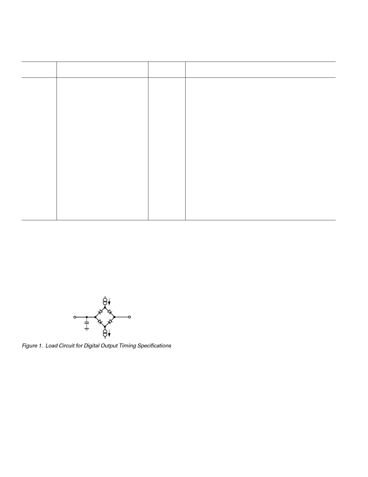
4Measured with the load circuit of Figure 1 and defined as the time required for the output to cross 0.8 V or 1.8 V when V DD = 2.35 V and 0.8 V or 2.0 V for VDD > 2.35 V.
5Measured with 50 pF load capacitor.
6t8 is derived from the measured time taken by the data outputs to change 0.5 V when loaded with the circuit of Figure 1. The measured number is then extrapolated
back to remove the effects of charging or discharging the 50 pF capacitor. This means that the time, t8, quoted in the timing characteristics is the true bus relinquish
time of the part and is independent of the bus loading.
7t7 values also apply to t8 minimum values.
8See Power-Up Time section.
Specifications subject to change without notice.
200A
IOL
TO OUTPUT
PIN CL
50pF
200A
IOH
1.6V
Figure 1. Load Circuit for Digital Output Timing Specifications
–6–
REV. C
Share Link: 