MXED102 データシートの表示(PDF) - Clare Inc => IXYS
部品番号
コンポーネント説明
メーカー
MXED102 Datasheet PDF : 20 Pages
| |||
Preliminary
MXED102
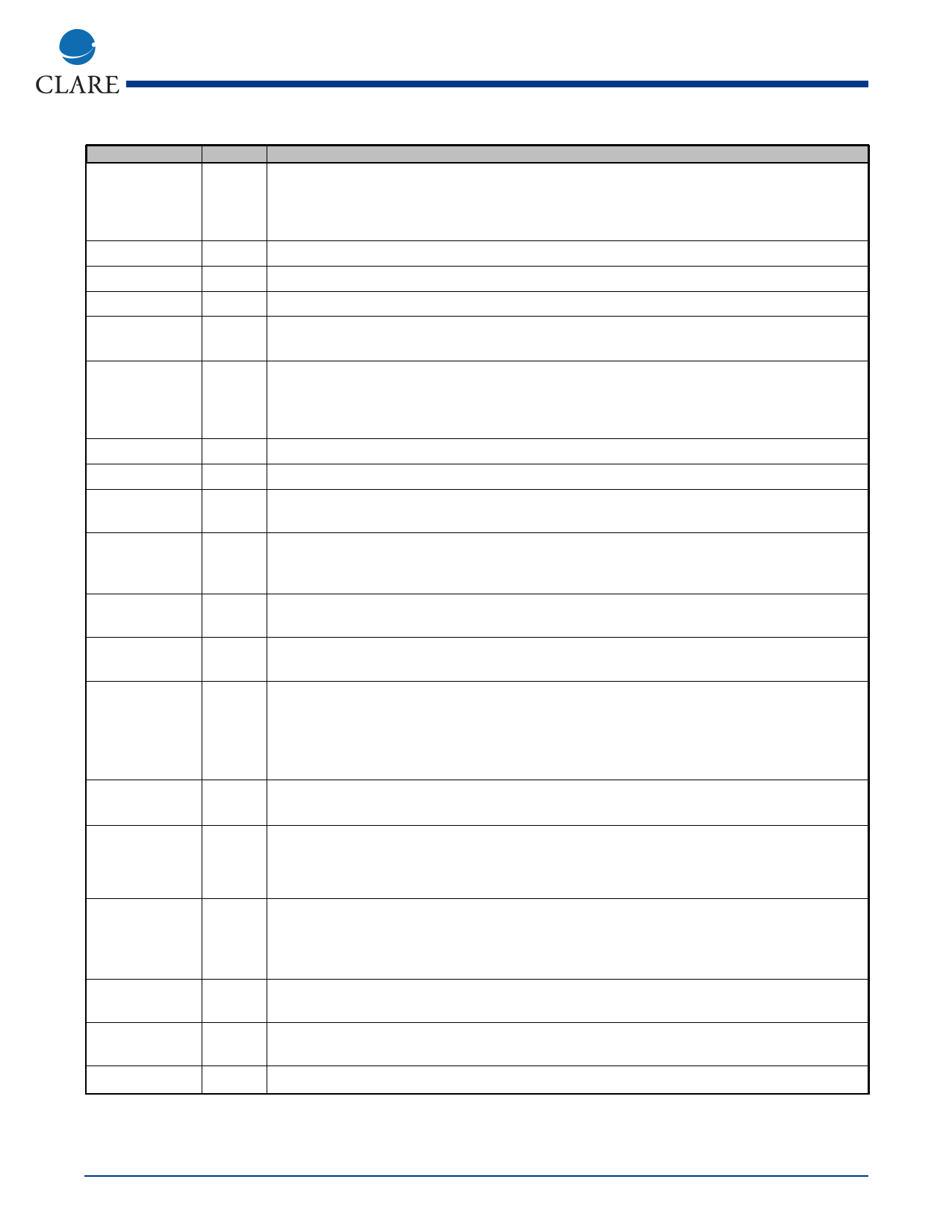
Pin List
Name
VDDA,
VDDB,
VDDC
VCC
GND
GNDA
ISHRT
I/O/A
-
-
-
-
-
PRECHA,
O/A
PRECHB,
PRECHC
MASTER_IN
I
MASTER_OUT O
RSTB
I
CLKSH
I
LTKNB
I/O
RTKNB
I/O
DIRTKN
I
LE
I
DA(5-0),
I
DB(5-0),
DC(5-0)
CLKEX
I
CLKSER
I
SDATA
I/O
SAMPLE
I
Description
High voltage supply A/B/C:
Logic supply:
Ground:
Analog ground:
Ground used to short output channels: There can be high currents on this line. It
should be separated from the circuit ground pads (GND) to prevent ground bounce.
Precharge A/B/C: Column precharge voltage outputs. PRECHA/B/C should be tied
to PRECHA/B/C of all other column drivers to ensure a uniform display precharge
and should be bypassed to ground with a capacitor at least 50 times the display
capacitance.
Master In: High input implies chip is master. This input is pulled low internally.
Master Out: MASTER_IN delayed by 1 LE clock cycle, sampled on rising edge of LE.
Reset Bar: Input signal used to reset digital logic for test purposes. This input is
pulled high internally.
Token Shift Clock: Input signal used to shift tokens down the length of the driver IC
and latch data into the corresponding columns. The direction of token shift is deter
mined by DIRTKN pin.
Left Token Bit: Input for shift right, output for shift left. Signal is used to pass the
tokens into and out of the driver IC. High state represents the presence of token.
Right Token Bit: Input for shift left, output for shift right. Signal is used to pass the
tokens into and out of the driver IC. High state represents the presence of token.
Token Direction Input: Input signal which, when high, causes the token to shift left to
right in the driver IC. A low signal causes the token to shift right to left. In the paral
lel data mode the token passes through the chip in 80 CLKSH clocks, in the serial
data mode the token passes through the chip in 240 CLKSH clocks. This input is
pulled high internally.
Latch Enable: Input signal used to begin data output. When data output begins, new
data input for the following row can begin.
Data A/B/C: Signal buses used to input the exposure data.
Exposure Clock: Input signal used to clock the driver IC's exposure counter from 0 to
63 for a row exposure. The signal must be cycled at least 64 times between LE
pulses to completely cycle the counter. Cycles of CLKEX beyond 64 will have no
effect.
Serial Clock: Clock to write serial data into all column drivers or read serial data from
the master column driver.
Serial Data: Serial data written to all column drivers or read from the master column
driver.
Initiate A/D sample. This input is pulled low internally.
Rev. 2
www.clare.com
3
Share Link: 