MSM6882-3 データシートの表示(PDF) - Oki Electric Industry
部品番号
コンポーネント説明
メーカー
MSM6882-3 Datasheet PDF : 15 Pages
| |||
¡ Semiconductor
MSM6882-3/6882-5
Name
AI
CDT
CDO
RD
RT
CF
CT
FT
VDD
Description
Receive analog signal input.
AI is biased internally to SG with about 100 kW same as TI.
Device test.
This pin should be connected to GND.
Device test.
This pin should be opened.
Demodulated serial data output.
This data is synchronized with the re-generated timing clock RT.
Receive data timing clock output.
This signal is re-generated by internal digital PLL.
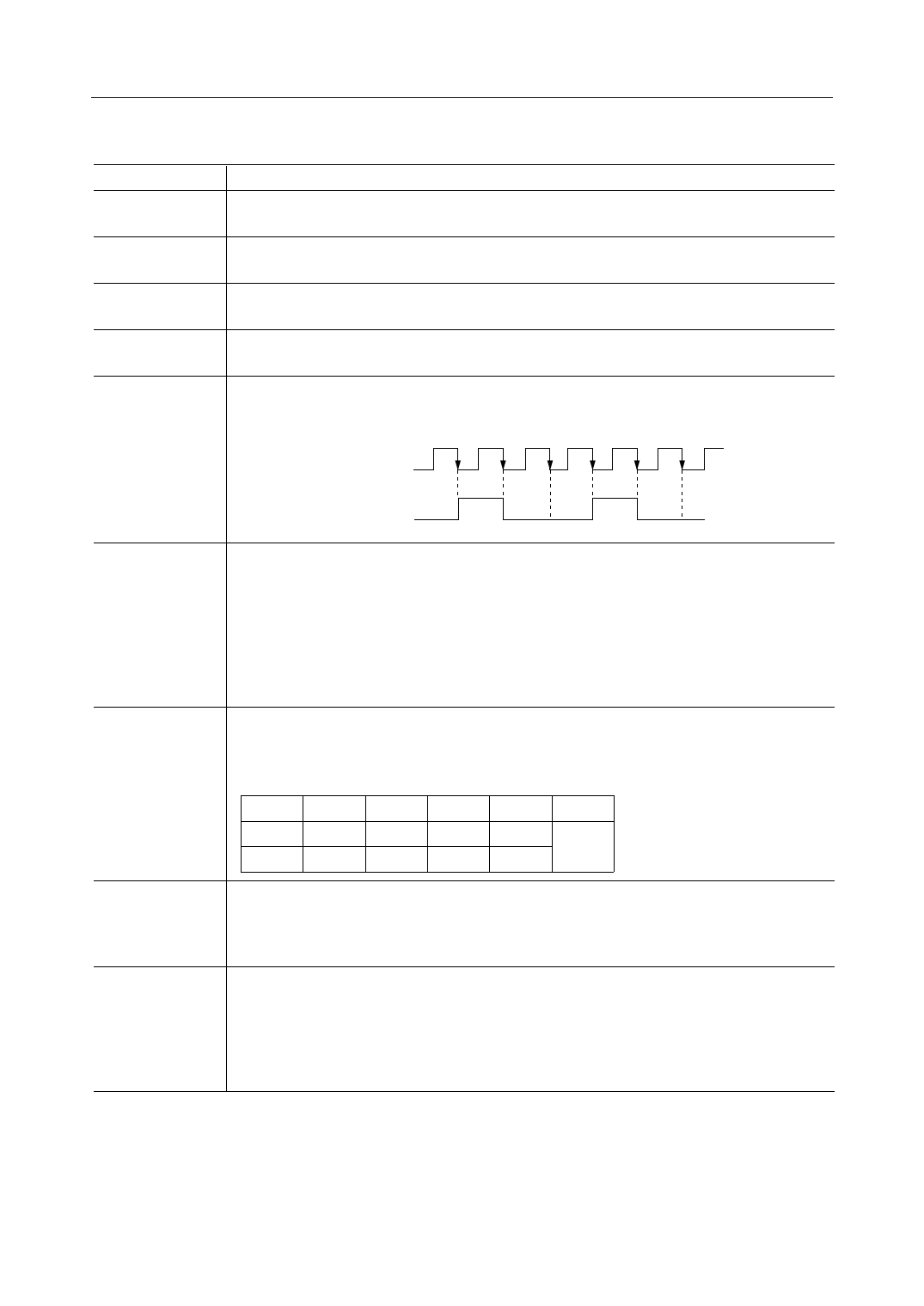
Synchronizing to negative edge of RT, RD is output.
RT
RD
Receive data timing clock is re-generated by digital PLL of which phase correcting speed can
be selected with CF.
When a digital "1" is put on CF and phase difference between receive data timing and RT is
more than 22.5 degree, phase correcting speed is high. In this case, as the phase difference
enters within 22.5 degrees, that speed changes to low immediately.
When digital "0" is input to CF, phase correcting speed of PLL remains low regardless of the
phase difference.
Usually, CF is connected to digital "1".
PLL's lock-in characteristics can be selected with CT.
When digital "1" is put on CT, PLL requires max. 50 bit alternative data pattern. On the other
hand, when digital "0" is input to CT,
PLL can be locked in below 18-bit data.
CF
CT MIN TYP MAX UNIT
1
0
—
—
18
bit
1
1
—
—
50
Control signal for the internal connection of AO.
Refer to column AO.
When digital "0" is input to this pin, transmit LPF enters in power down mode, but the output
buffer operational amplifier remains active. In this case, AO is at SG level.
Power supply.
MSM6882-3: 3.6 V
MSM6882-5: 5 V
This device is sensitive to supply noise as switched capacitor techniques are utilized.
A bypass capacitor of more than 2.2 mF between VDD and GND is indispensable to ensure the
performance.
6/15
Share Link: 