AD9139(Rev0) データシートの表示(PDF) - Analog Devices
部品番号
コンポーネント説明
メーカー
AD9139 Datasheet PDF : 56 Pages
| |||
AD9139
Data Sheet
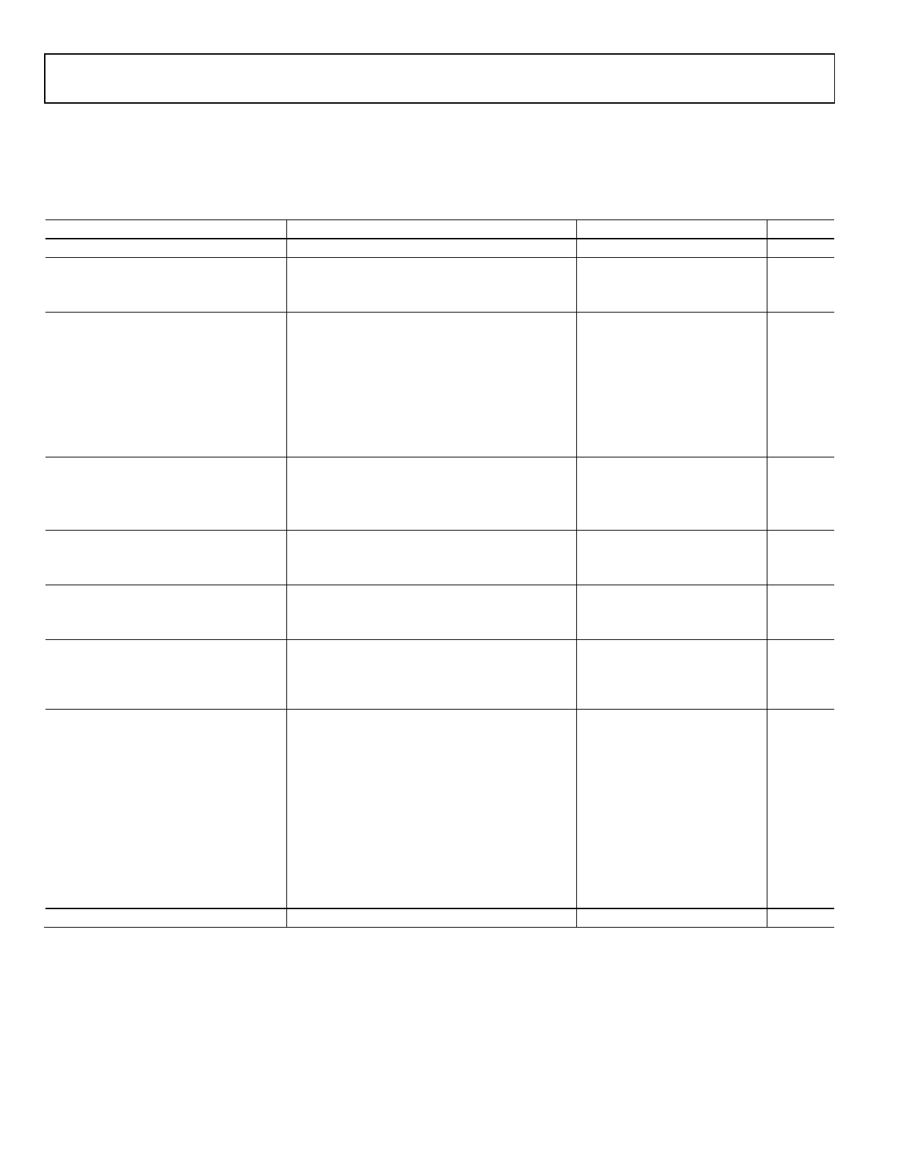
SPECIFICATIONS
DC SPECIFICATIONS
TMIN to TMAX, AVDD33 = 3.3 V, DVDD18 = 1.8 V, CVDD18 = 1.8 V, IOUTFS = 20 mA, maximum sample rate, unless otherwise noted.
Table 1.
Parameter
RESOLUTION
ACCURACY
Differential Nonlinearity (DNL)
Integral Nonlinearity (INL)
MAIN DAC OUTPUT
Offset Error
Gain Error
Full-Scale Output Current
Output Compliance Range
Output Resistance
Gain DAC Monotonicity
Settling Time to Within ±0.5 LSB
MAIN DAC TEMPERATURE DRIFT
Offset
Gain
Reference Voltage
REFERENCE
Internal Reference Voltage
Output Resistance
ANALOG SUPPLY VOLTAGES
AVDD33
CVDD18
DIGITAL SUPPLY VOLTAGES
DVDD18
DVDD18 Variation over Operating
Conditions1
POWER CONSUMPTION
1× Mode
2× Mode
Phase-Locked Loop
Inverse Sinc
Reduced Power Mode (Power-Down)
AVDD33 Current
CVDD18 Current
DVDD18 Current
OPERATING RANGE
Test Conditions/Comments
With internal reference
10 kΩ external resistor between FSADJ and AVSS
fDAC = 614 MSPS
fDAC = 1230 MSPS
fDAC = 800 MSPS
fDAC = 1600 MSPS
fDAC = 1230 MSPS
Min
Typ
16
Max
Unit
Bits
±2.1
LSB
±3.7
LSB
−0.001
−3.2
19.06
−1.0
0
+0.001
+2
+4.7
19.8
20.6
+1.0
10
Guaranteed
20
% FSR
% FSR
mA
V
MΩ
ns
0.04
ppm/°C
100
ppm/°C
30
ppm/°C
1.17
5
1.19
V
kΩ
3.13
3.3
1.7
1.8
3.47
V
1.9
V
1.7
1.8
−2.5%
1.9
V
+2.5% V
440
mW
700
mW
670
mW
1150
mW
70
mW
60
mW
57.3
mW
0.4
mA
26.6
mA
4.5
mA
−40
+25
+85
°C
1 This parameter specifies the maximum allowable variation of DVDD18 over operating conditions compared with the DVDD18 presented to the device at the time the
data interface DLL is enabled.
Rev. 0 | Page 4 of 56
Share Link: 