AD9444 データシートの表示(PDF) - Analog Devices
部品番号
コンポーネント説明
メーカー
AD9444 Datasheet PDF : 40 Pages
| |||
AD9444
Table 9. Reference Configuration Summary
Selected Mode
SENSE Voltage
External Reference
AVDD
Internal Fixed Reference
VREF
Programmable Reference
0.2 V to VREF
Internal Fixed Reference
AGND to 0.2 V
Resulting VREF (V)
N/A
0.5
0.5
×
⎜⎛1 +
⎝
R2
R1
⎟⎞
⎠
(See Figure
41)
1.0
Resulting Differential Span (V p-p)
2 × External Reference
1.0
2 × VREF
2.0
External Reference Operation
The AD9444’s internal reference is trimmed to enhance the gain
accuracy of the ADC. An external reference may be more stable
over temperature, but the gain of the ADC is not likely to be
improved. Figure 36 shows the typical drift characteristics of the
internal reference in both 1 V and 0.5 V modes.
When the SENSE pin is tied to AVDD, the internal reference is
disabled, allowing the use of an external reference. An internal
reference buffer loads the external reference with an equivalent
7 kΩ load. The internal buffer still generates the positive and
negative full-scale references, REFT and REFB, for the ADC
core. The input span is always twice the value of the reference
voltage; therefore, the external reference must be limited to a
maximum of 1 V.
Analog Inputs
As with most new high speed, high dynamic range ADCs, the
analog input to the AD9444 is differential. Differential inputs
improve on-chip performance as signals are processed through
attenuation and gain stages. Most of the improvement is a result
of differential analog stages having high rejection of even-order
harmonics. There are also benefits at the PCB level. First,
differential inputs have high common-mode rejection of stray
signals, such as ground and power noise. Second, they provide
good rejection of common-mode signals, such as local oscillator
feedthrough. The specified noise and distortion of the AD9444
cannot be realized with a single-ended analog input, so such
configurations are discouraged. Contact ADI for recommenda-
tions of other 14-bit ADCs that support single-ended analog
input configurations.
With the 1 V reference (nominal value, see the Internal Refer-
ence Trim section), the differential input range of the AD9444’s
analog input is nominally 2 V p-p or 1 V p-p on each input
(VIN+ or VIN−).
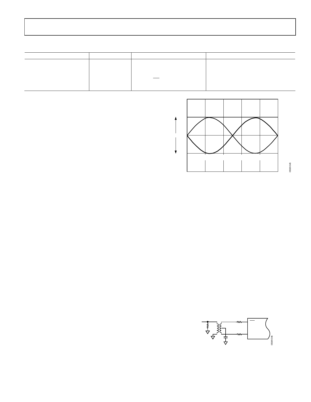
VIN+
1Vp-p
VIN–
DIGITAL OUT = ALL 1s
3.5V
DIGITAL OUT = ALL 0s
Figure 42. Differential Analog Input Range for VREF = 1 V
The AD9444 analog input voltage range is offset from ground
by 3.5 V. Each analog input connects through a 1 kΩ resistor to
the 3.5 V bias voltage and to the input of a differential buffer.
The internal bias network on the input properly biases the
buffer for maximum linearity and range (see the Equivalent
Circuits section). Therefore, the analog source driving the
AD9444 should be ac-coupled to the input pins. The recom-
mended method for driving the analog input of the AD9444 is
to use an RF transformer to convert single-ended signals to
differential (see Figure 44). Series resistors between the output
of the transformer and the AD9444 analog inputs help isolate
the analog input source from switching transients caused by the
internal sample-and-hold circuit. The series resistors, along with
the 1 kΩ resisters connected to the internal 3.5 V bias, must be
considered in impedance matching the transformers input. For
example, if RT were set to 51 Ω and RS were set to 33 Ω, along
with a 1:1 impedance ratio transformer, the input would match
a 50 Ω source with a full-scale drive of 10.0 dBm. The 50 Ω
impedance matching can also be incorporated on the secondary
side of the transformer, as shown in the evaluation board sche-
matic (see Figure 47 and Figure 59).
ANALOG
INPUT
SIGNAL RT
ADT1–1WT
RS
RS
0.1µF
AIN
AD9444
AIN
Figure 43. Transformer-Coupled Analog Input Circuit
Rev. 0 | Page 21 of 40
Share Link: 