AD9617JR-REEL データシートの表示(PDF) - Analog Devices
部品番号
コンポーネント説明
メーカー
AD9617JR-REEL Datasheet PDF : 10 Pages
| |||
AD9617
AC GAIN CHARACTERISTICS
Closed-loop bandwidth at high frequencies is determined pri-
marily by the roll-off of T(s). But circuit layout is critical to
minimize external parasitics which can degrade performance by
causing premature peaking and/or reduced bandwidth.
The inverting and noninverting dynamic characteristics are similar.
When driving the noninverting input, the inverting input capaci-
tance (CI) will cause the noninverting closed-loop bandwidth to
be higher than the inverting bandwidth for gains less than two
(2). In the remaining cases, inverting and noninverting responses
are nearly identical.
For best overall dynamic performance, the value of the feedback
resistor (RF) should be 400 ohms. Although bandwidth reduces
as closed-loop gain increases, the change is relatively small due
to low equivalent series input impedance, ZS. (See typical
performance charts.) The simplified equations governing the
device’s dynamic performance are shown below.
Closed-Loop Gain vs. Frequency:
(noninverting operation)
VO ≈
1 + RF
RI
+1
VI
s1 +
RS
(6)
RI
where: = RF × CC = 0.9 ns (RF = 400 Ω)
Slew Rate ≈ ∆VO × e−τ/RF KCC
RF KCC
(7)
where:
K
=1+
RS
RI
Increasing Bandwidth at Low Gains
By reducing RF, wider bandwidth and faster pulse response can
be attained beyond the specified values, although increased
overshoot, settling time and possible ac peaking may result. As a
rule of thumb, overshoot and bandwidth will increase by 1%
and 8%, respectively, for a 5% reduction in RF at gains of ± 10.
Lower gains will increase these sensitivities.
Equations 6 and 7 are simplified and do not accurately model
the second order (open loop) frequency response term which is
the primary contributor to overshoot, peaking and nonlinear
bandwidth expansion. (See Open Loop Bode Plots.) The user
should exercise caution when selecting RF values much lower
than 400 Ω. Note that a feedback resistor must be used in all
situations, including those in which the amplifier is used in a
noninverting unity gain configuration.
Increasing Bandwidth at High Gains
Closed loop bandwidth can be extended at high closed loop gain
by reducing RF. Bandwidth reduction is a result of the feedback
current being split between RS and RI. As the gain increases (for
a given RF), more feedback current is shunted through RI, which
reduces closed loop bandwidth (see Equation 6). To maintain
specified BW, the following equations can be used to approxi-
mate RF and RI for any gain from ± l to ± 15.
RF = 424 ± 8 G
(8)
(+ for inverting and – for noninverting)
RI
≈
424 − 8 G
G −1
(noninverting) (9)
RI
≈
424 + 8 G
G −1
(inverting) (10)
G = Closed Loop Gain.
Bandwidth Reduction
The closed loop bandwidth can be reduced by increasing RF.
Equations 6 and 7 can be used to determine the closed loop
bandwidth for any value RF. Do not connect a feedback capaci-
tor across RF, as this will degrade dynamic performance and
possibly induce oscillation.
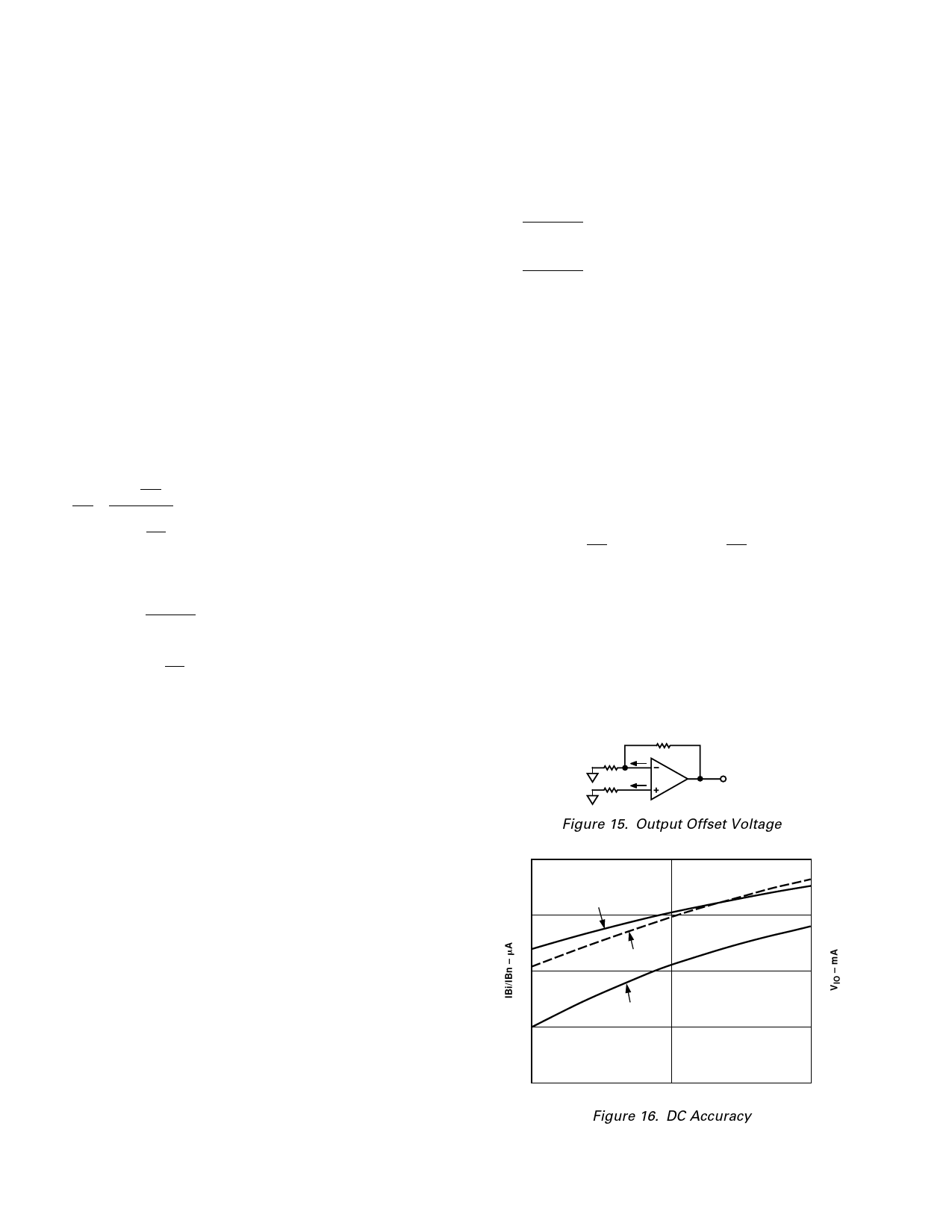
DC Precision and Noise
Output offset voltage results from both input bias currents and
input offset voltage. These input errors are multiplied by the
noise gain term (1 + RF/RI) and algebraically summed at the
output as shown below.
VO
=
V
IO
×
1
+
RF
RI
± IBn × RN
×
1
+
RF
RI
± IBi × RF
(11)
Since the inputs are asymmetrical, IBi and IBn do not correlate.
Canceling their output effects by making RN = RFʈRI will not
reduce output offset errors, as it would for voltage feedback
amplifiers. Typically, IBn is 5 µA and VIO is +0.5 mV (I sigma =
0.3 mV), which means that the dc output error can be reduced
by making RN ≈ 100 Ω. Note that the offset drift will not change
significantly because the IBn TC is relatively small. (See specifi-
cation table.)
RF
RI IBi
RN IBn
VOUT
Figure 15. Output Offset Voltage
10
1.0
IBn
5
0.5
VIO
0
0
IBi
–5
–0.5
–10
–55؇C
25؇C
Figure 16. DC Accuracy
–1.0
125؇C
–8–
REV. B
Share Link: 