AD9895KBC データシートの表示(PDF) - Analog Devices
部品番号
コンポーネント説明
メーカー
AD9895KBC Datasheet PDF : 58 Pages
| |||
AD9891/AD9895
SPECIFICATION DEFINITIONS
Differential Nonlinearity (DNL)
An ideal ADC exhibits code transitions that are exactly 1 LSB
apart. DNL is the deviation from this ideal value. Thus, every
code must have a finite width. No missing codes guaranteed to
12-bit resolution indicates that all 4096 codes, respectively,
must be present over all operating conditions.
Peak Nonlinearity
Peak nonlinearity, a full signal chain specification, refers to the
peak deviation of the output of the AD9891/AD9895 from a
true straight line. The point used as “zero scale” occurs 0.5 LSB
before the first code transition. “Positive full scale” is defined as
a level 1 and 0.5 LSB beyond the last code transition. The
deviation is measured from the middle of each particular output
code to the true straight line. The error is then expressed as a
percentage of the 2 V ADC full-scale signal. The input signal is
always appropriately gained up to fill the ADC’s full-scale range.
Total Output Noise
The rms output noise is measured using histogram techniques. The
standard deviation of the ADC output codes is calculated in LSB
and represents the rms noise level of the total signal chain at the
specified gain setting. The output noise can be converted to an
equivalent voltage, using the relationship 1 LSB = (ADC Full
Scale/2n codes) when n is the bit resolution of the ADC. For the
AD9891, 1 LSB is 2 mV, while for the AD9895, 1 LSB is 0.5 mV.
Power Supply Rejection (PSR)
The PSR is measured with a step change applied to the supply
pins. The PSR specification is calculated from the change in the
data outputs for a given step change in the supply voltage.
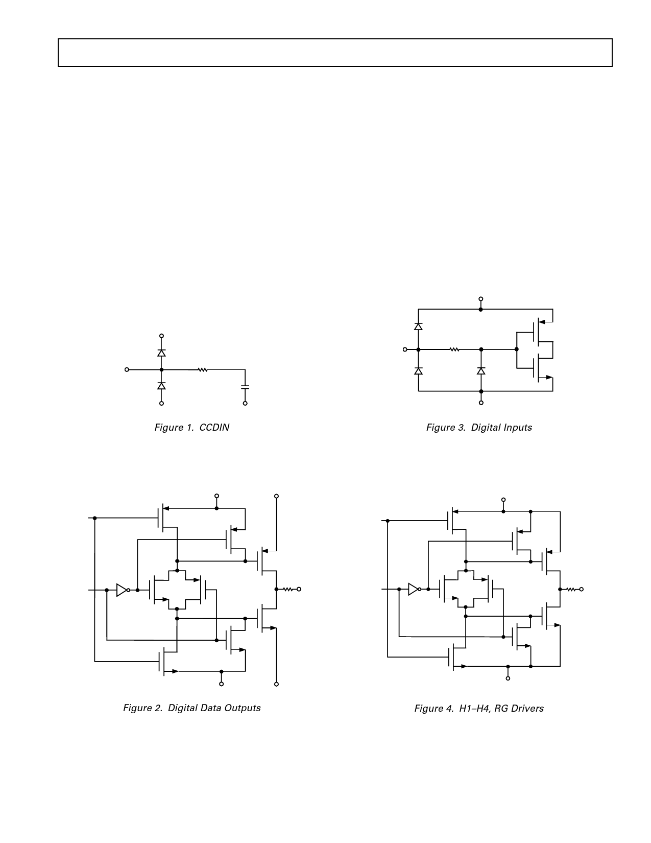
EQUIVALENT CIRCUITS
DVDD
AVDD1
R
330⍀
AVSS1
AVSS1
Figure 1. CCDIN
DVSS
Figure 3. Digital Inputs
DATA
DVDD
DRVDD
RG, H1–H4
HVDD OR
RGVDD
THREE-
STATE
DOUT
ENABLE
OUTPUT
DVSS
DRVSS
Figure 2. Digital Data Outputs
HVSS OR
RGVSS
Figure 4. H1–H4, RG Drivers
REV. A
–9–
Share Link: 