AD9923A(Rev0) データシートの表示(PDF) - Analog Devices
部品番号
コンポーネント説明
メーカー
AD9923A Datasheet PDF : 88 Pages
| |||
AD9923A
Parameter
BLACK LEVEL CLAMP
Clamp Level Resolution
Minimum Clamp Level (Code 0)
Maximum Clamp Level (Code 1023)
ANALOG-TO-DIGITAL CONVERTER (ADC)
Resolution
Differential Nonlinearity (DNL)
No Missing Codes
Full-Scale Input Voltage
VOLTAGE REFERENCE
Reference Top Voltage (REFT)
Reference Bottom Voltage (REFB)
SYSTEM PERFORMANCE
Gain Accuracy
Low Gain (VGA Code 15)
Maximum Gain (VGA Code 1023)
Peak Nonlinearity, 500 mV Input Signal
Total Output Noise
Power Supply Rejection (PSR)
Conditions/Comments
Measured at ADC output
Includes entire signal chain
Default CDS gain (0 dB)
12 dB gain applied
AC-grounded input, 6 dB gain applied
Measured with step change on supply
Min Typ
Max Unit
1024
0
255
Steps
LSB
LSB
12
Bits
−1.0 ±0.5
+1.0 LSB
Guaranteed
2.0
V
2.0
V
1.0
V
6.0 6.5
42.0 42.5
0.1
1.0
50
7.0 dB
43.0 dB
%
LSB rms
dB
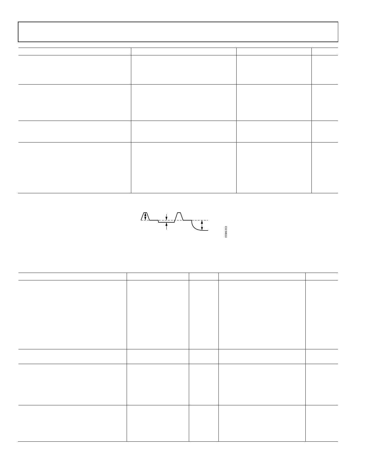
1 Input signal characteristics are defined as shown in Figure 3.
1V MAX
INPUT SIGNAL RANGE
(0dB CDS GAIN)
500mV TYP
RESET TRANSIENT
200mV MAX
OPTICAL BLACK PIXEL
TIMING SPECIFICATIONS
Figure 3. Signal Characteristics
CL = 20 pF, AVDD = DVDD = DRVDD = 3.0 V, fCLI = 36 MHz, unless otherwise noted.
Table 6.
Parameter
MASTER CLOCK, CLI
CLI Clock Period
CLI High/Low Pulse Width
Delay from CLI Rising Edge to Internal Pixel Position 0
AFE CLPOB Pulse Width1, 2
Allowable Region for HD Falling Edge to CLI Rising Edge
SHP Inhibit Region
AFE SAMPLE LOCATION1
SHP Sample Edge to SHD Sample Edge
DATA OUTPUTS
Output Delay from DCLK Rising Edge1
Inhibited Area for DOUTPHASE Edge Location
Pipeline Delay from SHP/SHD Sampling to Data Output
SERIAL INTERFACE
Maximum SCK Frequency
SL to SCK Setup Time
SCK to SL Hold Time
SDATA Valid to SCK Rising Edge Setup
SCK Falling Edge to SDATA Valid Hold
SCK Falling Edge to SDATA Valid Read
Conditions/Comments Symbol Min Typ Max
Unit
tCONV
tCLIDLY
Only valid in slave mode tHDCLI
Only valid in slave mode tSHPINH
27.8
11.2 13.9 16.6
6
2 20
4
tCONV − 2
30
39
ns
ns
ns
Pixels
ns
Edge location
tS1
11.6 13.9
ns
tOD
8
ns
SHD
SHD + 11 Edge location
16
Cycles
fSCLK
36
tLS
10
tLH
10
tDS
10
tDH
10
tDV
10
MHz
ns
ns
ns
ns
ns
1 Parameter is programmable.
2 Minimum CLPOB pulse width is for functional operation only. Wider typical pulses are recommended to achieve good clamp performance.
Rev. 0 | Page 6 of 88
Share Link: 