AD9925 データシートの表示(PDF) - Analog Devices
部品番号
コンポーネント説明
メーカー
AD9925 Datasheet PDF : 96 Pages
| |||
AD9925
TIMING SPECIFICATIONS
CL = 20 pF, AVDD = DVDD = DRVDD = 3.0 V, fCLI = 36 MHz, unless otherwise noted.
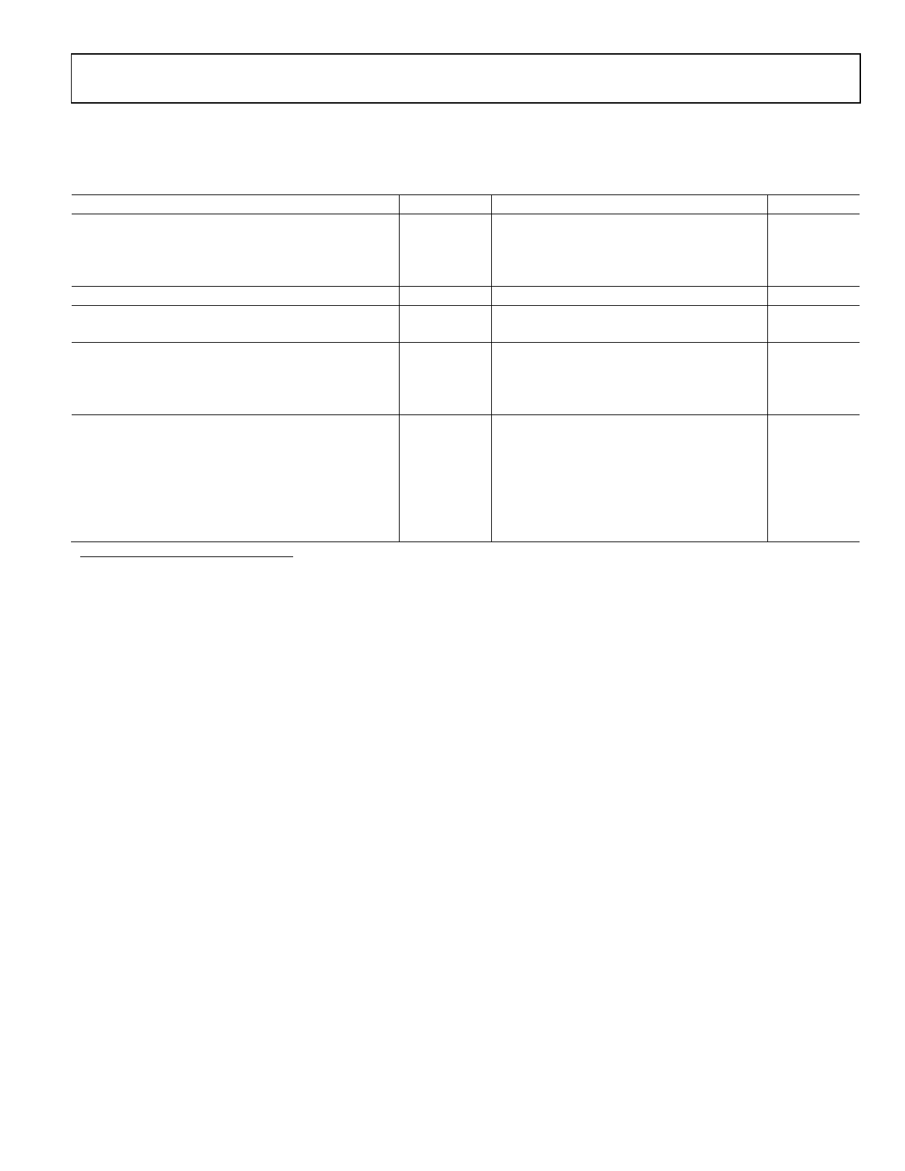
Table 5.
Parameter
MASTER CLOCK, CLI (Figure 17)
CLI Clock Period
CLI High/Low Pulse Width
Delay from CLI Rising Edge to Internal Pixel Position 0
AFE CLPOB PULSE WIDTH1, 2 (Figure 23 and Figure 29)
AFE SAMPLE LOCATION1 (Figure 20)
SHP Sample Edge to SHD Sample Edge
DATA OUTPUTS (Figure 21 and Figure 22)
Output Delay from DCLK Rising Edge, Default Value1
Inhibited Area for DOUTPHASE Edge Location1
Pipeline Delay from SHP/SHD Sampling to DOUT
SERIAL INTERFACE (Figure 74 and Figure 75)
Maximum SCK Frequency
SL to SCK Setup Time
SCK to SL Hold Time
SDATA Valid to SCK Rising Edge Setup
SCK Falling Edge to SDATA Valid Hold
SCK Falling Edge to SDATA Valid Read
Symbol
tCONV
tCLIDLY
tS1
tOD
tDOUTINH
fSCLK
tLS
tLH
tDS
tDH
tDV
Min
Typ
27.8
11.2
13.9
6
2
20
12.5
13.9
8
SHDLOC
11
36
10
10
10
10
10
Max
Unit
ns
16.6
ns
ns
Pixels
ns
SHDLOC + 11
ns
Cycles
MHz
ns
ns
ns
ns
ns
1 Parameter is register-programmable.
2 Minimum CLPOB pulse width is for functional operation only. Wider typical pulses are recommended to achieve good clamp performance.
Rev. A | Page 7 of 96
Share Link: 