AD9929 データシートの表示(PDF) - Analog Devices
部品番号
コンポーネント説明
メーカー
AD9929 Datasheet PDF : 64 Pages
| |||
AD9929
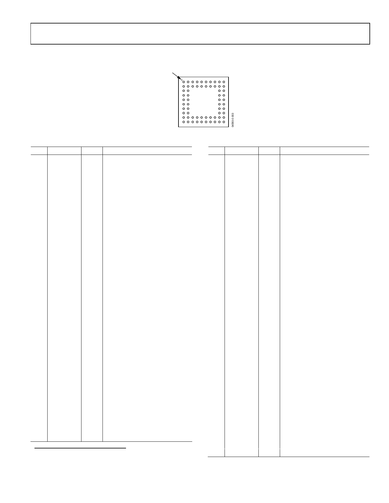
PIN CONFIGURATION AND FUNCTIONAL DESCRIPTIONS
A 1 CORNER
INDEX AREA
1 2 3 4 5 6 7 8 9 10
A
B
C
D
AD9929
E
F
TOP VIEW
G
(Not to Scale)
H
J
K
Figure 2. Pin Configuration
Table 7. Pin Function Descriptions
Pin Mnemonic Type1 Description
D1 VD
DIO
Vertical Sync Pulse (Input for Slave
Mode, Output for Master Mode)
D2 HD
Horizontal Sync Pulse (Input for
DIO Slave Mode, Output for Master
Mode)
B8 D0
DO Data Output
A8 D1
DO Data Output
A7 D2
DO Data Output
B7 D3
DO Data Output
A6 D4
DO Data Output
B6 D5
DO Data Output
B5 D6
DO Data Output
A4 D7
DO Data Output
B3 D8
DO Data Output
A3 D9
DO Data Output
B2 D10
DO Data Output
A2 D11
DO Data Output
A1 DCLK1
DO Data Clock Output
B4 DRVSS
P
Data Output Driver Ground
A5 DRVDD
P
Data Output Driver Supply
G9 SUBCK
DO
CCD Substrate Clock
(2 Level: VH2, VL)
D10 V1
DO
CCD Vertical Transfer Clock
(3 Level: VH1, VM1, VL)
E9 V2
DO
CCD Vertical Transfer Clock
(2 Level: VM2, VL)
G10 V3
DO
CCD Vertical Transfer Clock
(3 Level: VH1, VM1, VL)
H9 V4
DO
CCD Vertical Transfer Clock
(2 Level: VM2, VL)
H10 VH1
P
Vertical Driver High Supply
(High Supply for V1 and V3)
C10 VM1
P
Vertical Driver Midsupply
(Midsupply for V1 and V3)
F10 VM2
P
Vertical Driver Midsupply
(Midsupply for V2 and V4)
F9 VL
P
Vertical Driver Low Supply
E10 VH2
P
Vertical Driver High Supply for
SUBCK
1 AI = Analog Input, AO = Analog Output, DI = Digital Input,
DO = Digital Output, DIO = Digital Input/Output, P = Power.
Pin Mnemonic Type1 Description
B10 VDD
P
Vertical Driver Input Logic Supply
J9 VDVSS
P
Vertical Driver Ground
A9 VSUB
DO CCD Substrate Bias
G1 H1
DO CCD Horizontal Clock
F1 H2
DO CCD Horizontal Clock
E1 HVDD
P
H1 and H2 Driver Supply
E2 HVSS
P
H1 and H2 Driver Ground
F2 HVSS
P
H1 and H2 Driver Ground
G2 HVSS
P
H1 and H2 Driver Ground
H1 RG
DO CCD Reset Gate Clock
J1 RGVDD
P
RG Driver Supply
H2 RGVSS
P
RG Driver Ground
C9
SYNC or
VGATE
DI
DI
External System Sync Input
VGATE Input
C1
FD or
DCLK2
DO Field Designator Output
DO DCLK2 Output
K3 AVDD
P
Analog Supply for AFE
J3 AVSS
P
Analog Ground for AFE
J4 AVSS
P
Analog Ground for AFE
J5 AVSS
P
Analog Ground for AFE
J6 AVSS
P
Analog Ground for AFE
J7 AVSS
P
Analog Ground for AFE
J8 AVSS
P
Analog Ground for AFE
K4 AVSS
P
Analog Ground for AFE
K6 AVSS
P
Analog Ground for AFE
J2 CLI
DI
Reference Clock Input
K2 TCVDD
P
Analog Supply for Timing Core
K1 TCVSS
P
Analog Ground for Timing Core
K5 CCDIN
AI
CCD Input Signal
K7 REFT
AO Voltage Reference Top Bypass
K8 REFB
AO Voltage Reference Bottom Bypass
K9 SDATA
DI
3-Wire Serial Data Input
K10 SL
DI
3-Wire Serial Load Pulse
J10 SCK
DI
3-Wire Serial Clock
D9 OUTCONT DI
Output Control
B1 MSHUT
DO Mechanical Shutter Pulse
C2 STROBE
DO Strobe Pulse
A10 DVDD
P
Digital Supply
B9 DVSS
P
Digital Ground
Rev. A | Page 9 of 64
Share Link: 