AD9937 データシートの表示(PDF) - Analog Devices
部品番号
コンポーネント説明
メーカー
AD9937 Datasheet PDF : 44 Pages
| |||
AD9937
ANALOG SPECIFICATIONS (AVDD = 3 V, fCLI = 12 MHz, –25؇C to +85؇C, unless otherwise noted.)
Parameter
Min
Typ
Max Unit
Notes
CDS
Allowable CCD Reset Transient
500
Max Input Range before Saturation
1.0
Max CCD Black Pixel Amplitude
± 100
mV
V p-p
mV
Input signal characteristics.*
VARIABLE GAIN AMPLIFIER (VGA)
Max Output Range
2.0
Gain Control Resolution
Gain Monotonicity
Gain Range
Low Gain (VGA Code 0)
Max Gain (VGA Code 1023)
40
10
Guaranteed
5.3
41.1
V p-p
Bits
dB
dB
BLACK LEVEL CLAMP
Clamp Level Resolution
Clamp Level
Min Clamp Level
Max Clamp Level
255
0
63.75
Steps
LSB
LSB
LSB measured at ADC output.
A/D CONVERTER
Resolution
Differential Nonlinearity (DNL)
No Missing Codes
Full-Scale Input Voltage
10
Bits
± 0.4
± 1.0 LSB
Guaranteed
2.0
V
VOLTAGE REFERENCE
Reference Top Voltage (REFT)
2.0
V
Reference Bottom Voltage (REFB)
1.0
V
SYSTEM PERFORMANCE
Gain Accuracy
Low Gain (VGA Code 17)
5
6
Max Gain (VGA Code 1023)
40.2
41.2
Peak Nonlinearity, 500 mV Input Signal
0.1
Total Output Noise
0.3
Power Supply Rejection (PSR)
40
Includes entire signal chain.
7
dB
Gain = (0.035 × Code) + 5.4 dB
42.2 dB
%
12 dB gain applied.
LSB rms AC ground input, 6 dB gain applied.
dB
Measured with step change on supply.
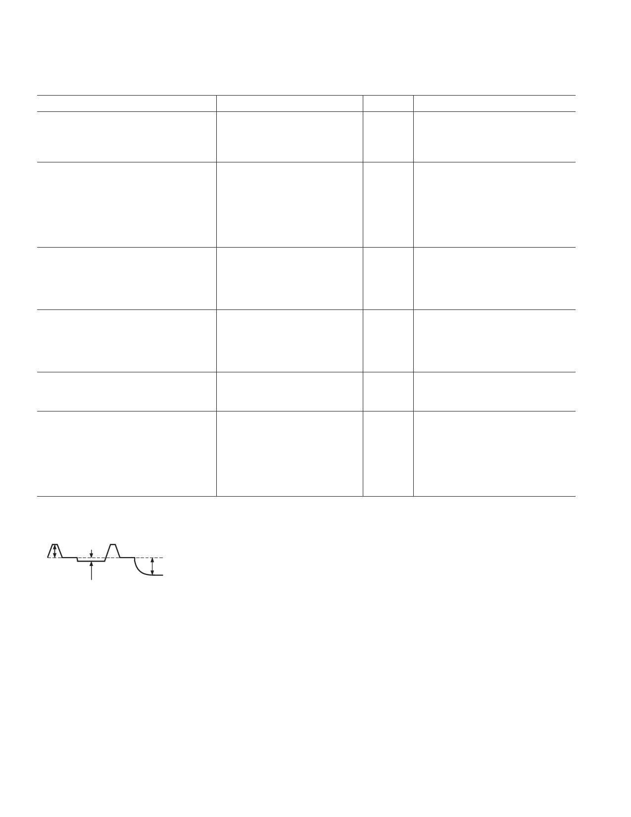
*Input signal characteristics defined as follows:
500mV TYP
RESET
TRANSIENT
100mV MAX
OPTICAL
BLACK PIXEL
1V MAX
INPUT
SIGNAL RANGE
Specifications subject to change without notice.
–4–
REV. 0
Share Link: 