AD9944(RevC) データシートの表示(PDF) - Analog Devices
部品番号
コンポーネント説明
メーカー
AD9944 Datasheet PDF : 20 Pages
| |||
Data Sheet
Parameter
VOLTAGE REFERENCE
Reference Top Voltage (REFT)
Reference Bottom Voltage (REFB)
SYSTEM PERFORMANCE
Gain Range
Low Gain (VGA Code = 0)
Maximum Gain (VGA Code = 1023)
Gain Accuracy
Peak Nonlinearity 500 mV Input Signal
Total Output Noise
Power Supply Rejection (PSR)
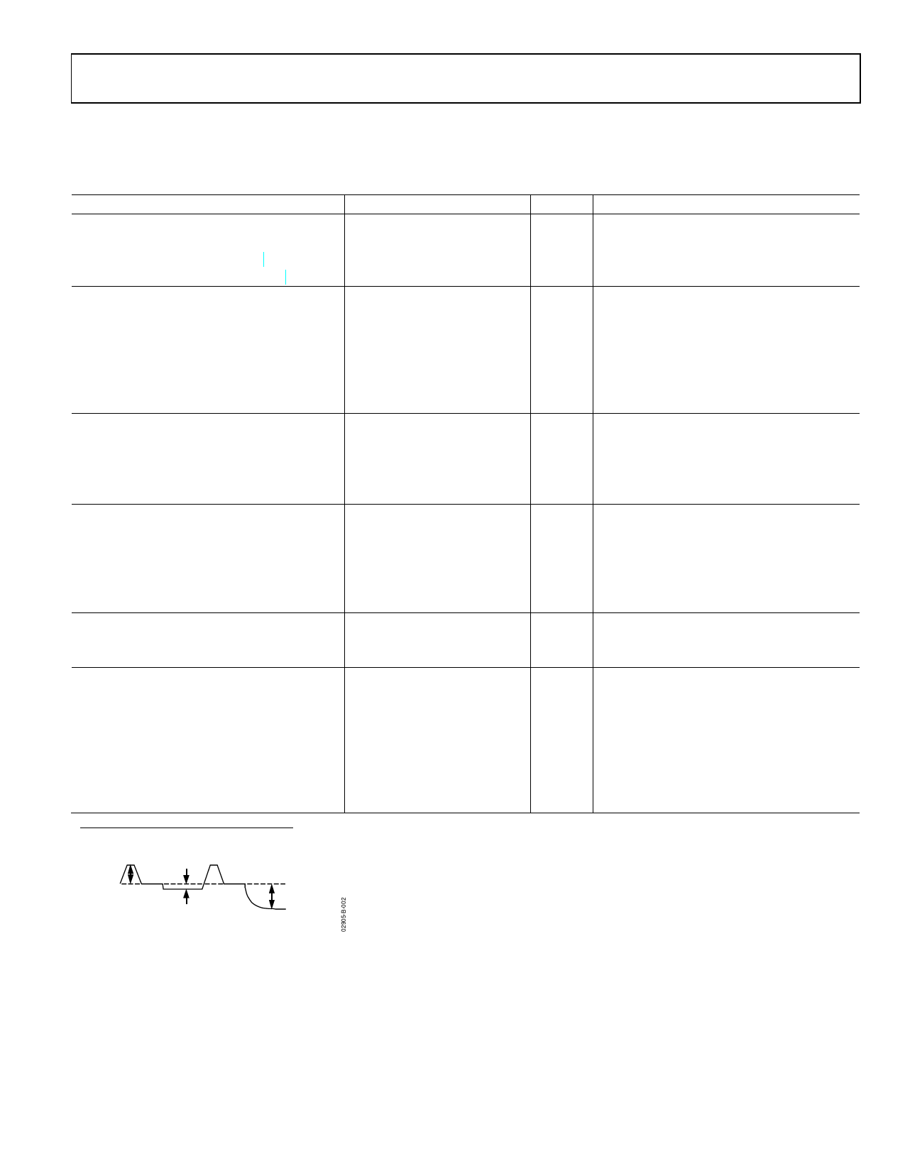
1 Input signal characteristics defined as follows:
Min Typ
2.0
1.0
5.3
40 41.5
±1
0.1
0.9
50
500mV TYP
RESET TRANSIENT
100mV TYP
OPTICAL BLACK PIXEL
1V TYP
INPUT SIGNAL RANGE
AD9943/AD9944
Max Unit
Conditions
V
V
Specifications include entire signal chain.
dB
dB
dB
%
LSB rms
dB
12 dB gain applied.
AC grounded input, 6 dB gain applied.
Measured with step change on supply.
TIMING SPECIFICATIONS
CL = 20 pF, fSAMP = 25 MHz. See CCD-mode timing in Figure 14 and Figure 15, and serial timing in Figure 10 and Figure 11.
Table 4.
Parameter
SAMPLE CLOCKS
DATACLK, SHP, SHD Clock Period
DATACLK High/Low Pulse Width
SHP Pulse Width
SHD Pulse Width
CLPOB Pulse Width1
SHP Rising Edge to SHD Falling Edge
SHP Rising Edge to SHD Rising Edge
Internal Clock Delay
DATA OUTPUTS
Output Delay
Pipeline Delay
SERIAL INTERFACE
Maximum SCK Frequency
SL to SCK Setup Time
SCK to SL Hold Time
SDATA Valid to SCK Rising Edge Setup
SCK Falling Edge to SDATA Valid Hold
Symbol
tCONV
tADC
tSHP
tSHD
tCOB
tS1
tS2
tID
tOD
fSCLK
tLS
tLH
tDS
tDH
Min
Typ
Max
Unit
40
16
20
10
10
2
20
10
16
20
3.0
ns
ns
ns
ns
Pixels
ns
ns
ns
9.5
ns
9
Cycles
10
MHz
10
ns
10
ns
10
ns
10
ns
1 Minimum CLPOB pulse width is for functional operation only. Wider typical pulses are recommended to achieve low noise clamp performance.
Rev. C | Page 5 of 20
Share Link: 