AD9944 データシートの表示(PDF) - Analog Devices
部品番号
コンポーネント説明
メーカー
AD9944 Datasheet PDF : 20 Pages
| |||
AD9943/AD9944
AD9943 SYSTEM SPECIFICATIONS
TMIN to TMAX, AVDD = DVDD = DRVDD = 3 V, fSAMP = 25 MHz, unless otherwise noted.
Table 3.
Parameter
CDS
Maximum Input Range before Saturation1
Allowable CCD Reset Transient1
Maximum CCD Black Pixel Amplitude1
VARIABLE GAIN AMPLIFIER (VGA)
Gain Control Resolution
Gain Monotonicity
Gain Range
Minimum Gain
Maximum Gain
Min Typ
1.0
500
100
1024
Guaranteed
5.3
40 41.5
Max Unit
V p-p
mV
mV
Steps
dB
dB
BLACK LEVEL CLAMP
Clamp Level Resolution
Clamp Level
Minimum Clamp Level
Maximum Clamp Level
A/D CONVERTER
Resolution
Differential Nonlinearity (DNL)
No Missing Codes
Data Output Coding
Full-Scale Input Voltage
VOLTAGE REFERENCE
Reference Top Voltage (REFT)
Reference Bottom Voltage (REFB)
SYSTEM PERFORMANCE
Gain Range
Low Gain (VGA Code = 0)
Maximum Gain (VGA Code = 1023)
Gain Accuracy
Peak Nonlinearity 500 mV Input Signal
Total Output Noise
Power Supply Rejection (PSR)
256
0
63.75
10
±0.3
Guaranteed
Straight binary
2.0
2.0
1.0
5.3
40 41.5
±1
0.1
0.3
50
Steps
LSB
LSB
Bits
LSB
V
V
V
dB
dB
dB
%
LSB rms
dB
Conditions
See input waveform in footnote.
See Figure 13 for VGA gain curve.
See Variable Gain Amplifier section for VGA
gain equation.
Measured at ADC output.
Specifications include entire signal chain.
12 dB gain applied.
AC grounded input, 6 dB gain applied.
Measured with step change on supply.
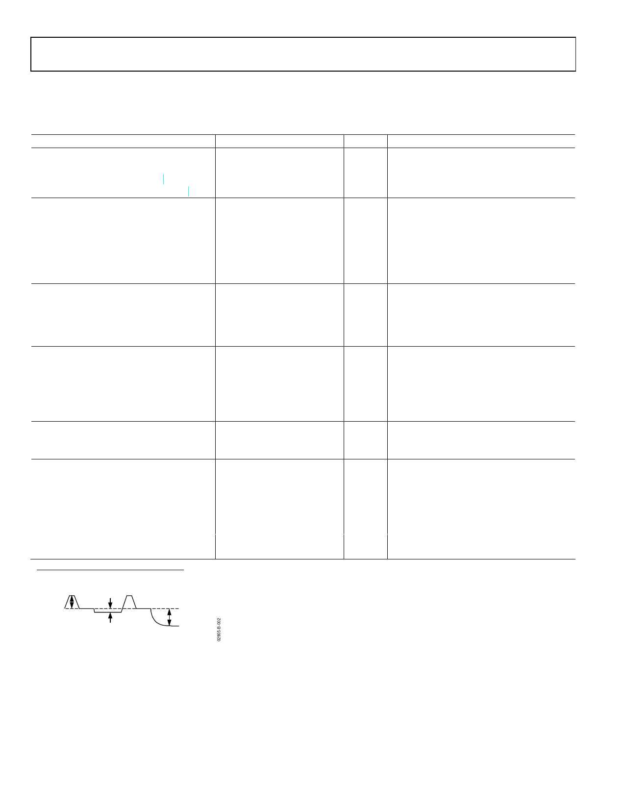
1 Input signal characteristics defined as follows:
500mV TYP
RESET TRANSIENT
100mV TYP
OPTICAL BLACK PIXEL
1V TYP
INPUT SIGNAL RANGE
Rev. B | Page 4 of 20
Share Link: 