AD9944 データシートの表示(PDF) - Analog Devices
部品番号
コンポーネント説明
メーカー
AD9944 Datasheet PDF : 20 Pages
| |||
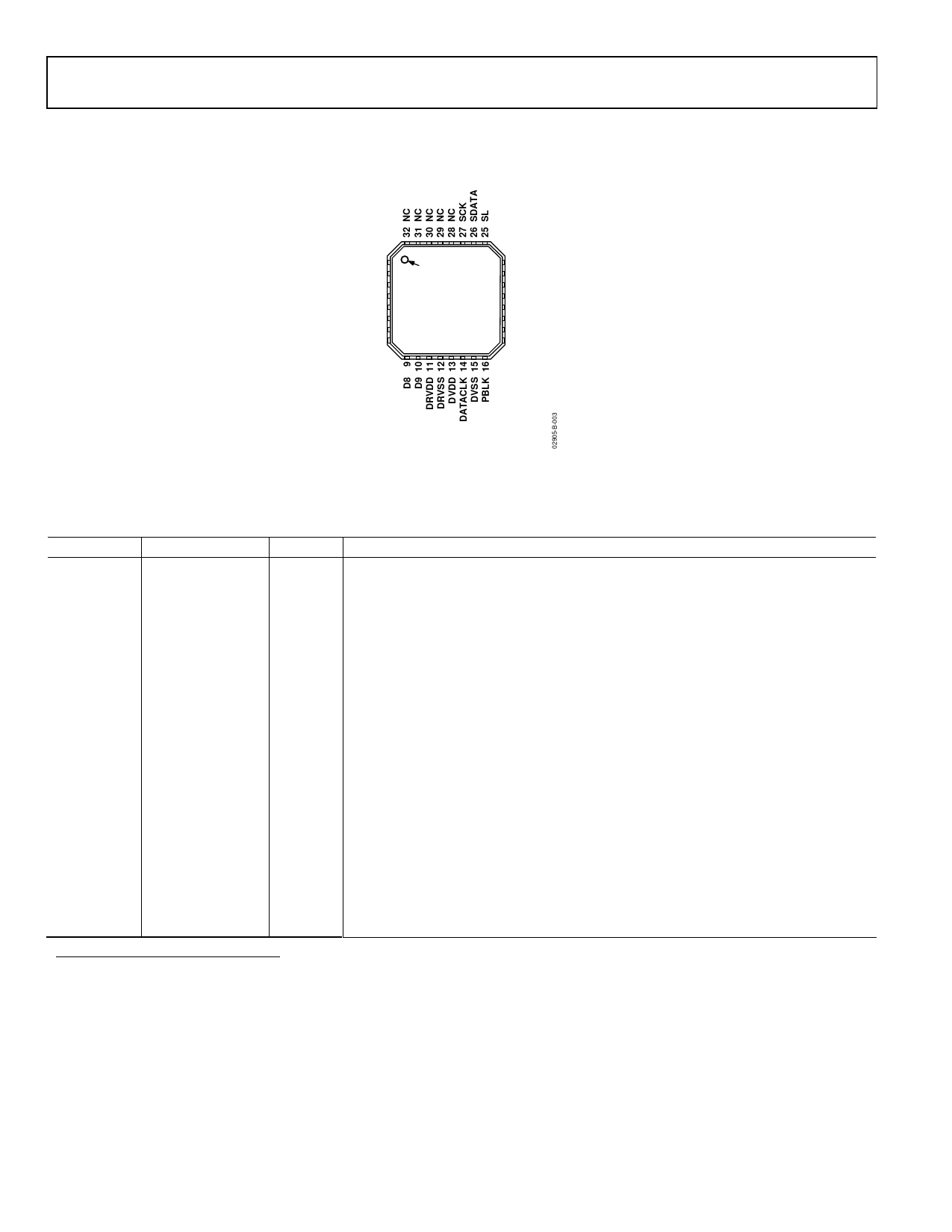
AD9943/AD9944
AD9943 PIN CONFIGURATION AND FUNCTION DESCRIPTIONS
D0 1
D1 2
D2 3
D3 4
D4 5
D5 6
D6 7
D7 8
PIN 1
INDICATOR
AD9943
TOP VIEW
24 REFB
23 REFT
22 CCDIN
21 AVSS
20 AVDD
19 SHD
18 SHP
17 CLPOB
NC = NO CONNECT
Figure 2. AD9943 Pin Configuration
Table 7. AD9943 Pin Function Descriptions
Pin No.
Mnemonic
Type1
1 to 10
D0 to D9
DO
11
DRVDD
P
12
DRVSS
P
13
DVDD
P
14
DATACLK
DI
15
DVSS
P
16
PBLK
DI
17
CLPOB
DI
18
SHP
DI
19
SHD
DI
20
AVDD
P
21
AVSS
P
22
CCDIN
AI
23
REFT
AO
24
REFB
AO
25
SL
DI
26
SDATA
DI
27
SCK
DI
28 to 30
NC
NC
31 to 32
NC
NC
Description
Digital Data Outputs.
Digital Output Driver Supply.
Digital Output Driver Ground.
Digital Supply.
Digital Data Output Latch Clock.
Digital Supply Ground.
Preblanking Clock Input.
Black Level Clamp Clock Input.
CDS Sampling Clock for CCD Reference Level.
CDS Sampling Clock for CCD Data Level.
Analog Supply.
Analog Ground.
Analog Input for CCD Signal.
A/D Converter Top Reference Voltage Decoupling.
A/D Converter Bottom Reference Voltage Decoupling.
Serial Digital Interface Load Pulse.
Serial Digital Interface Data Input.
Serial Digital Interface Clock Input.
Internally pulled down. Float or connect to GND.
Internally not nonnected.
1 Type: AI = analog input, AO = analog output, DI = digital input, DO = digital output, P = power, and NC = no connect.
Rev. B | Page 8 of 20
Share Link: 