AD9945(RevC) データシートの表示(PDF) - Analog Devices
部品番号
コンポーネント説明
メーカー
AD9945 Datasheet PDF : 14 Pages
| |||
AD9945
0.1F CCDIN
DC RESTORE
CDS
6dB TO 40dB
VGA
INTERNAL
VREF
2V FULL SCALE
12-BIT
12
ADC
DOUT
10
VGA GAIN
REGISTER
8-BIT
DAC
OPTICAL BLACK
CLAMP
DIGITAL
FILTERING
8
CLAMP LEVEL
REGISTER
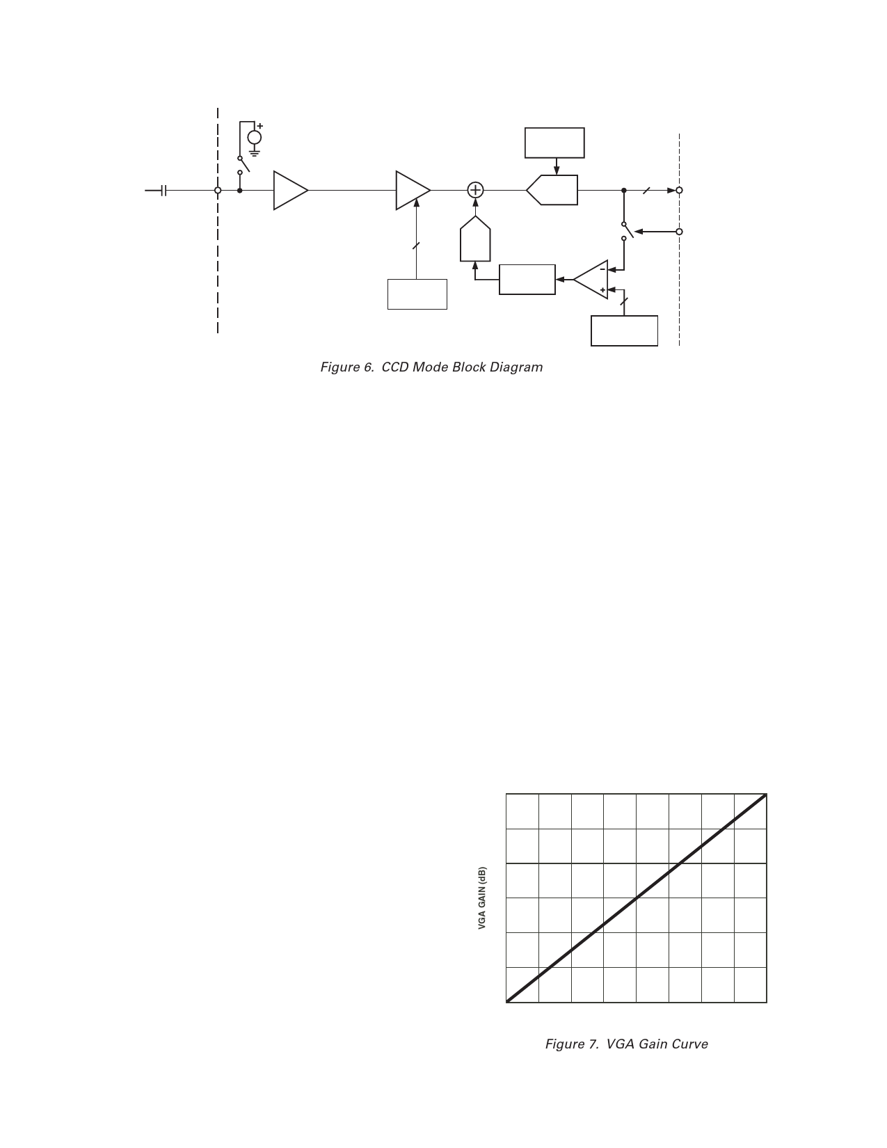
Figure 6. CCD Mode Block Diagram
CLPOB
CIRCUIT DESCRIPTION AND OPERATION
The AD9945 signal processing chain is shown in Figure 6. Each
processing step is essential in achieving a high quality image from
the raw CCD pixel data.
DC Restore
To reduce the large dc offset of the CCD output signal, a dc
restore circuit is used with an external 0.1 μF series coupling
capacitor. This restores the dc level of the CCD signal to
approximately 1.5 V to be compatible with the 3 V single supply
of the AD9945.
Correlated Double Sampler
The CDS circuit samples each CCD pixel twice to extract the
video information and reject low frequency noise. The timing
shown in Figure 8 illustrates how the two CDS clocks, SHP and
SHD, are used to sample the reference level and data level of
the CCD signal, respectively. The CCD signal is sampled on the
rising edges of SHP and SHD. Placement of these two clock
signals is critical in achieving the best performance from the CCD.
An internal SHP/SHD delay (tID) of 3 ns is caused by internal
propagation delays.
Optical Black Clamp
The optical black clamp loop is used to remove residual offsets
in the signal chain and to track low frequency variations in the
CCD’s black level. During the optical black (shielded) pixel
interval on each line, the ADC output is compared with the
fixed black level reference, selected by the user in the clamp
level register. The resulting error signal is filtered to reduce
noise, and the correction value is applied to the ADC input
through a D/A converter. Normally, the optical black clamp
loop is turned on once per horizontal line, but this loop can be
updated more slowly to suit a particular application. If external
digital clamping is used during the postprocessing, the AD9945
optical black clamping may be disabled using Bit D3 in the
operation register (see the Serial Interface Timing and Internal
Register Description sections).
When the loop is disabled, the clamp level register may still be
used to provide programmable offset adjustment.
Horizontal timing is shown in Figure 9. The CLPOB pulse should
be placed during the CCD’s optical black pixels. It is recom-
mended that the CLPOB pulse be used during valid CCD dark
pixels. The CLPOB pulse should be a minimum of 20 pixels wide
to minimize clamp noise. Shorter pulse widths may be used, but
clamp noise may increase and the loop’s ability to track low fre-
quency variations in the black level will be reduced.
A/D Converter
The ADC uses a 2 V input range. Better noise performance results
from using a larger ADC full-scale range. The ADC uses a
pipelined architecture with a 2 V full-scale input for low noise
performance.
Variable Gain Amplifier
The VGA stage provides a gain range of 6 dB to 40 dB, program-
mable with 10-bit resolution through the serial digital interface.
The minimum gain of 6 dB is needed to match a 1 V input signal
with the ADC full-scale range of 2 V. A plot of the VGA gain curve
is shown in Figure 7.
VGA Gain(dB) = (VGA Code × 0.035 dB) + 5.3 dB
42
36
30
24
18
12
6
0
127 255 383 511 639 767 895 1023
VGA GAIN REGISTER CODE
Figure 7. VGA Gain Curve
–10–
REV. C
Share Link: 