AD9945(RevC) データシートの表示(PDF) - Analog Devices
部品番号
コンポーネント説明
メーカー
AD9945 Datasheet PDF : 14 Pages
| |||
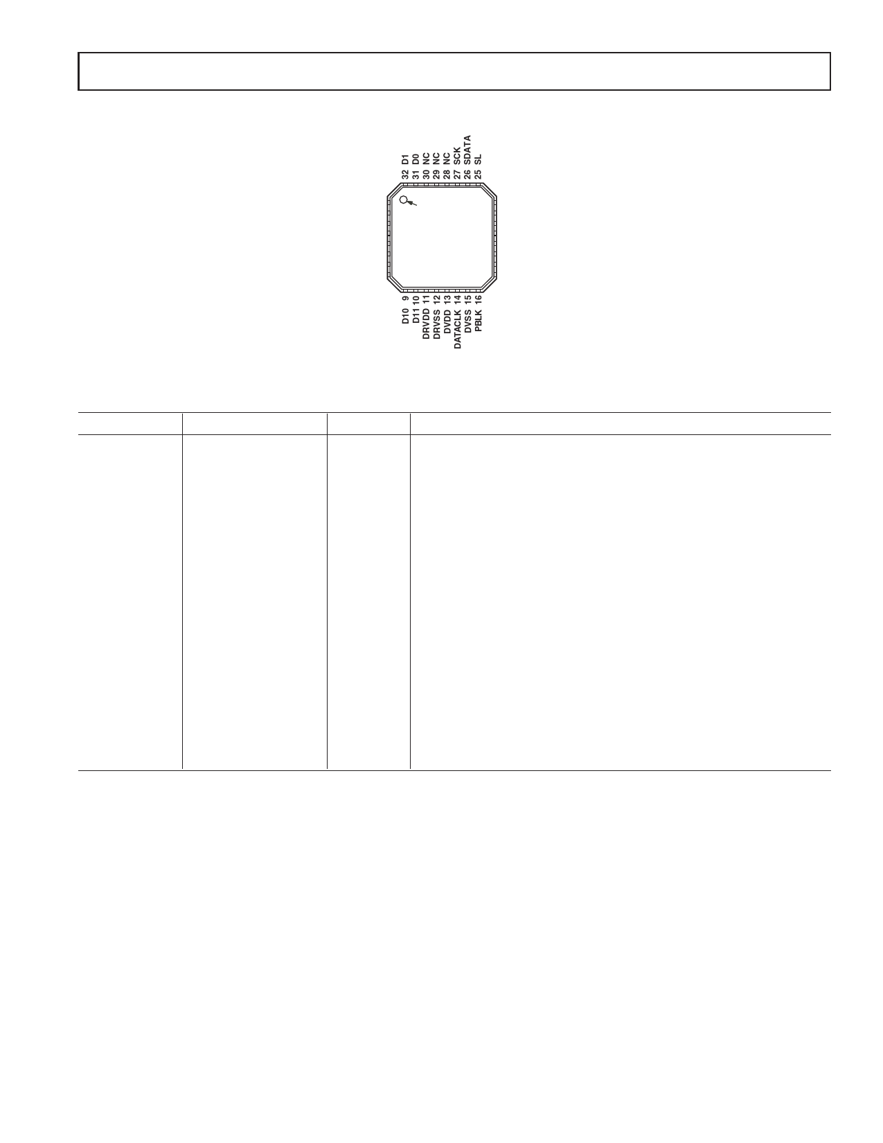
PIN CONFIGURATION
AD9945
D2 1
D3 2
D4 3
D5 4
D6 5
D7 6
D8 7
D9 8
PIN 1
INDICATOR
AD9945
TOP VIEW
24 REFB
23 REFT
22 CCDIN
21 AVSS
20 AVDD
19 SHD
18 SHP
17 CLPOB
NOTES
1. IT IS RECOMMENDED THAT THE EXPOSED PAD BE
SOLDERED TO THE GROUND PLANE OF THE PCB.
PIN FUNCTION DESCRIPTIONS
Pin Number
Mnemonic
Type
Description
1 to 10, 31, 32
11
12
13
14
15
16
17
18
19
20
21
22
23
24
25
26
27
28 to 30
D2 to D11, D0, D1 DO
DRVDD
P
DRVSS
P
DVDD
P
DATACLK
DI
DVSS
P
PBLK
DI
CLPOB
DI
SHP
DI
SHD
DI
AVDD
P
AVSS
P
CCDIN
AI
REFT
AO
REFB
AO
SL
DI
SDATA
DI
SCK
DI
NC
NC
Digital Data Outputs
Digital Output Driver Supply
Digital Output Driver Ground
Digital Supply
Digital Data Output Latch Clock
Digital Supply Ground
Preblanking Clock Input
Black Level Clamp Clock Input
CDS Sampling Clock for CCD’s Reference Level
CDS Sampling Clock for CCD’s Data Level
Analog Supply
Analog Ground
Analog Input for CCD Signal
A/D Converter Top Reference Voltage Decoupling
A/D Converter Bottom Reference Voltage Decoupling
Serial Digital Interface Load Pulse
Serial Digital Interface Data Input
Serial Digital Interface Clock Input
Internally Pulled Down. Float or connect to GND.
TYPE: AI = Analog Input, AO = Analog Output, DI = Digital Input, DO = Digital Output, P = Power.
REV. C
–5–
Share Link: 