AD9956 データシートの表示(PDF) - Analog Devices
部品番号
コンポーネント説明
メーカー
AD9956 Datasheet PDF : 32 Pages
| |||
AD9956
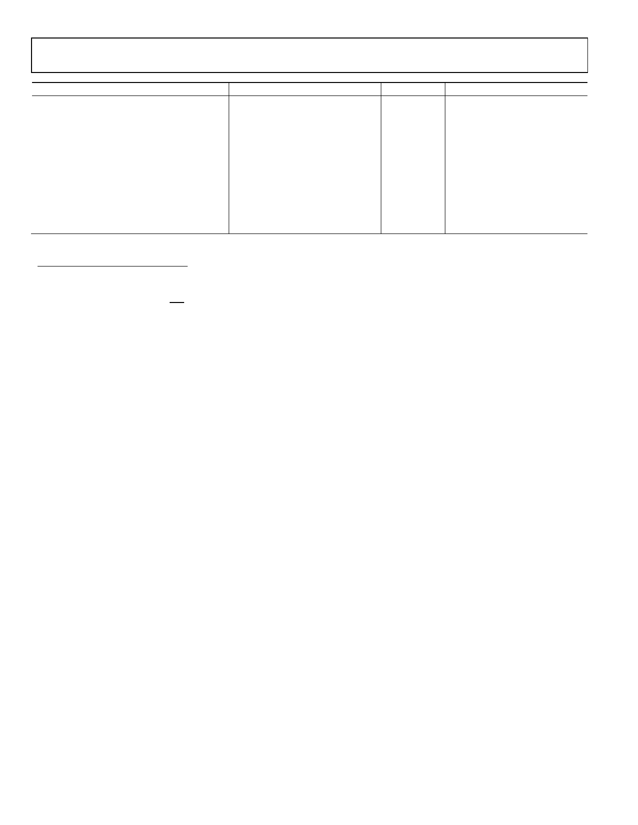
Parameter
Min
TOTAL SYSTEM JITTER AND PHASE NOISE FOR
105.33 MHz ADC CLOCK GENERATION CIRCUIT
Converter Limiting Jitter
Resultant SNR
Phase Noise of Fundamental
@ 10 Hz Offset
@ 100 Hz Offset
@ 1 kHz Offset
@ 10 kHz Offset
@ 100 kHz Offset
@ ≥1 MHz Offset
Typ Max
0.53
67
−75
−87
−93
−105
−145
−152
Unit
ps rms
dB
dBc/Hz
dBc/Hz
dBc/Hz
dBc/Hz
dBc/Hz
dBc/Hz
Test Conditions/Comments
See the Loop Measurement Condi-
tions section
1 The input impedance of the REFCLK input is 1500 Ω. However, in order to provide matching on the clock line, an external 50 Ω load is used.
2 Driving the PLLREF input buffer, the crystal oscillator section of this input stage performs up to only 30 MHz.
3 The charge pump output compliance range is functionally 0.2 V to (CP_VDD − 0.2 V). The value listed here is the compliance range for 5% matching.
4 Measured as peak-to-peak from DRV to DRV.
5 For a 4.02 kΩ resistor from DRV_RSET to GND.
6 Assumes a 1 mA load.
7 I/O_UPDATE/PS<2:0> are detected by the AD9956 synchronous to the rising edge of SYNC_CLK. Each latency measurement is from the first SYNC_CLK rising edge
after the I/O_UPDATE/PS<2:0> state change.
Rev. B | Page 8 of 32
Share Link: 