AD9995 データシートの表示(PDF) - Analog Devices
部品番号
コンポーネント説明
メーカー
AD9995 Datasheet PDF : 60 Pages
| |||
AD9995
PRECISION TIMING HIGH SPEED TIMING GENERATION CLIDIVIDE register (Addr. 0x30). The AD9995 will then inter-
The AD9995 generates high speed timing signals using the
nally divide the CLI frequency by 2.
flexible Precision Timing core. This core is the foundation for
The AD9995 also includes a master clock output, CLO, which is
generating the timing used for both the CCD and the AFE: the
the inverse of CLI. This output is intended to be used as a crystal
reset gate RG, horizontal drivers H1–H4, and SHP/SHD sample driver. A crystal can be placed between the CLI and CLO pins to
clocks. A unique architecture makes it routine for the system
generate the master clock for the AD9995. For more information
designer to optimize image quality by providing precise control
on using a crystal, see Figure 39.
over the horizontal CCD readout and the AFE correlated double
sampling.
High Speed Clock Programmability
Figure 5 shows how the high speed clocks RG, H1–H4, SHP,
The high speed timing of the AD9995 operates the same in either and SHD are generated. The RG pulse has programmable rising
Master or Slave mode configuration. For more information on
and falling edges, and may be inverted using the polarity control.
synchronization and pipeline delays, see the Power-Up and Syn-
The horizontal clocks H1 and H3 have programmable rising
chronization section.
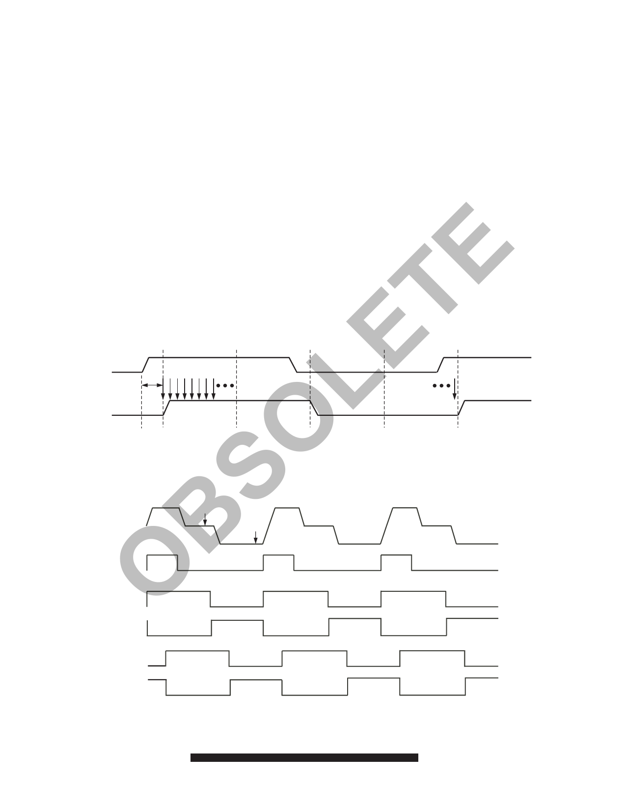
Timing Resolution
The Precision Timing core uses a 1 master clock input (CLI)
as a reference. This clock should be the same as the CCD pixel
clock frequency. Figure 4 illustrates how the internal timing core
divides the master clock period into 48 steps or edge positions.
E Using a 20 MHz CLI frequency, the edge resolution of the Preci-
sion Timing core is 1 ns. If a 1 system clock is not available, it
is also possible to use a 2 reference clock by programming the
and falling edges and polarity control. The H2 and H4 clocks
are always inverses of H1 and H3, respectively. Table I
summarizes the high speed timing registers and their parameters.
Figure 6 shows the typical 2-phase H-clock arrangement in
which H3 and H4 are programmed for the same edge location as
H1 and H2.
The edge location registers are 6 bits wide, but there are only 48
valid edge locations available. Therefore, the register values are
T POSITION
P[0]
CLI
E tCLIDLY
1 PIXEL
PERIOD
P[12]
P[24]
P[36]
P[48] = P[0]
L NOTES
PIXEL CLOCK PERIOD IS DIVIDED INTO 48 POSITIONS, PROVIDING FINE EDGE RESOLUTION FOR HIGH SPEED CLOCKS.
THERE IS A FIXED DELAY FROM THE CLI INPUT TO THE INTERNAL PIXEL PERIOD POSITIONS (tCLIDLY = 6ns TYP).
O Figure 4. High Speed Clock Resolution from CLI Master Clock Input
S CCD
SIGNAL
3
4
1
2
B RG
5
6
OH1
H2
7
8
H3
H4
PROGRAMMABLE CLOCK POSITIONS:
1. RG RISING EDGE
2. RG FALLING EDGE
3. SHP SAMPLE LOCATION
4. SHD SAMPLE LOCATION
5. H1 RISING EDGE POSITION
6. H1 FALLING EDGE POSITION (H2 IS INVERSE OF H1)
7. H3 RISING EDGE POSITION
8. H3 FALLING EDGE POSITION (H4 IS INVERSE OF H3)
Figure 5. High Speed Clock Programmable Locations
–10–
REV. 0
Share Link: 