AD9995KCPRL データシートの表示(PDF) - Analog Devices
部品番号
コンポーネント説明
メーカー
AD9995KCPRL Datasheet PDF : 60 Pages
| |||
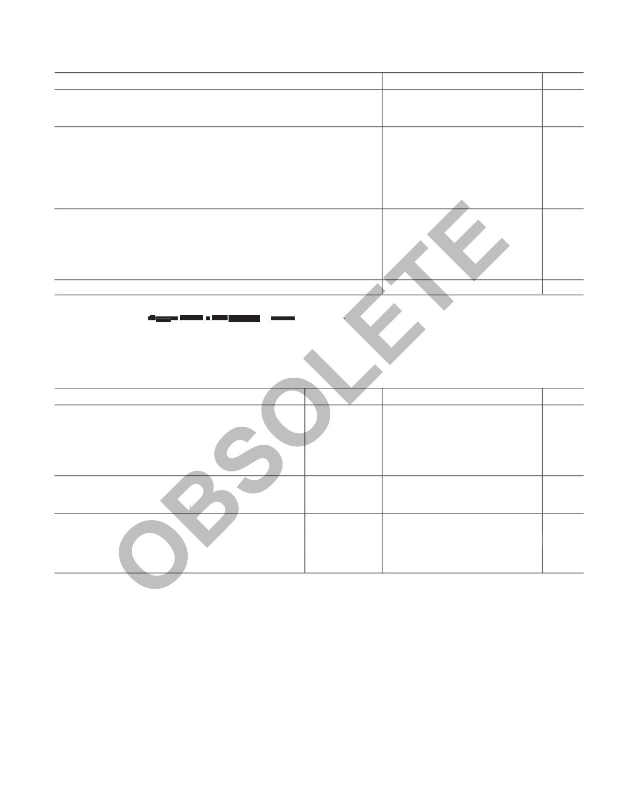
AD9995–SPECIFICATIONS
Parameter
Min
Typ
Max
TEMPERATURE RANGE
Operating
Storage
–20
+85
–65
+150
POWER SUPPLY VOLTAGE
AVDD (AFE Analog Supply)
TCVDD (Timing Core Analog Supply)
RGVDD (RG Driver)
HVDD (H1–H4 Drivers)
DRVDD (Data Output Drivers)
DVDD (Digital)
2.7
3.0
3.6
2.7
3.0
3.6
2.7
3.0
3.6
2.7
3.0
3.6
2.7
3.0
3.6
2.7
3.0
3.6
POWER DISSIPATION (See TPC 1 for Power Curves)
36 MHz, Typ Supply Levels, 100 pF H1–H4 Loading
Power from HVDD Only*
Standby 1 Mode
Standby 2 Mode
Standby 3 Mode
E MAXIMUM CLOCK RATE (CLI)
360
130
130
12
0.5
36
*The total power dissipated by the HVDD supply may be approximated using the equation
T [ ] Total HVDD Power = CLOAD × HVDD × Pixel Frequency × HVDD × Number of H−outputs used
Reducing the H-loading, using only two of the outputs, and/or using a lower HVDD supply will reduce the power dissipation.
Specifications subject to change without notice.
DIGITAL SPECIFICATIONS E Parameter
L LOGIC INPUTS
High Level Input Voltage
Low Level Input Voltage
High Level Input Current
O Low Level Input Current
Input Capacitance
LOGIC OUTPUTS (Except H and RG)
High Level Output Voltage @ IOH = 2 mA
S Low Level Output Voltage @ IOL = 2 mA
RG and H-DRIVER OUTPUTS (H1–H4)
High Level Output Voltage @ Max Current
Low Level Output Voltage @ Max Current
B Maximum Output Current (Programmable)
Maximum Load Capacitance (For Each Output)
O Specifications subject to change without notice.
Symbol
VIH
VIL
IIH
IIL
CIN
VOH
VOL
VOH
VOL
Min
Typ
Max
2.1
0.6
10
10
10
2.2
0.5
VDD – 0.5
0.5
30
100
Unit
°C
°C
V
V
V
V
V
V
mW
mW
mW
mW
mW
MHz
Unit
V
V
µA
µA
pF
V
V
V
V
mA
pF
REV. 0
–3–
Share Link: 