AD9995KCPRL データシートの表示(PDF) - Analog Devices
部品番号
コンポーネント説明
メーカー
AD9995KCPRL Datasheet PDF : 60 Pages
| |||
AD9995
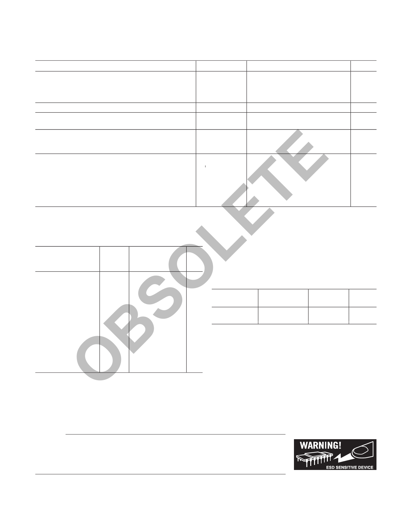
TIMING SPECIFICATIONS (CL = 20 pF, AVDD = DVDD = DRVDD = 3.0 V, fCLI = 36 MHz, unless otherwise noted.)
Parameter
Symbol
Min
Typ
Max
Unit
MASTER CLOCK, CLI (Figure 4)
CLI Clock Period
CLI High/Low Pulsewidth
Delay from CLI Rising Edge to Internal Pixel Position 0
tCONV
tCLIDLY
27.8
ns
11.2
13.9
16.6
ns
6
ns
AFE CLPOB Pulsewidth1, 2 (Figures 9 and 14)
2
20
Pixels
AFE SAMPLE LOCATION1 (Figure 7)
SHP Sample Edge to SHD Sample Edge
tS1
12.5
13.9
ns
DATA OUTPUTS (Figures 8a and 8b)
Output Delay from DCLK Rising Edge1
tOD
8
Pipeline Delay from SHP/SHD Sampling to DOUT
11
SERIAL INTERFACE (Figures 40a and 40b)
Maximum SCK Frequency
SL to SCK Setup Time
SCK to SL Hold Time
E SDATA Valid to SCK Rising Edge Setup
SCK Falling Edge to SDATA Valid Hold
SCK Falling Edge to SDATA Valid Read
fSCLK
10
tLS
10
tLH
10
tDS
10
tDH
10
tDV
10
T NOTES
1Parameter is programmable.
2Minimum CLPOB pulsewidth is for functional operation only. Wider typical pulses are recommended to achieve good clamp performance.
Specifications subject to change without notice.
ns
Cycles
MHz
ns
ns
ns
ns
ns
E ABSOLUTE MAXIMUM RATINGS*
L Parameter
With
Respect
To
Min Max
Unit
AVDD
AVSS –0.3 +3.9
V
TCVDD
TCVSS –0.3 +3.9
V
HVDD
HVSS –0.3 +3.9
V
O RGVDD
RGVSS –0.3 +3.9
V
DVDD
DVSS –0.3 +3.9
V
DRVDD
DRVSS –0.3 +3.9
V
RG Output
RGVSS –0.3 RGVDD + 0.3 V
S H1–H4 Output
HVSS –0.3 HVDD + 0.3 V
Digital Outputs
DVSS –0.3 DVDD + 0.3 V
Digital Inputs
DVSS –0.3 DVDD + 0.3 V
SCK, SL, SDATA
DVSS –0.3 DVDD + 0.3 V
B REFT, REFB, CCDIN AVSS
–0.3 AVDD + 0.3 V
Junction Temperature
150
°C
Lead Temperature, 10 sec
350
°C
*Stresses above those listed under Absolute Maximum Ratings may cause permanent
O damage to the device. This is a stress rating only. Functional operation of the device
PACKAGE THERMAL CHARACTERISTICS
Thermal Resistance
JA = 25°C/W*
*JA is measured using a 4-layer PCB with the exposed paddle soldered to the
board.
Model
AD9995KCP
AD9995KCPRL
ORDERING GUIDE
Temperature
Range
Package
Description
–20°C to +85°C LFCSP
–20°C to +85°C LFCSP
Package
Option
CP-56
CP-56
at these or any other conditions above those listed in the operational sections of
this specification is not implied. Exposure to absolute maximum rating conditions
for extended periods may affect device reliability. Absolute maximum ratings apply
individually only, not in combination. Unless otherwise specified, all other voltages
are referenced to GND.
CAUTION
ESD (electrostatic discharge) sensitive device. Electrostatic charges as high as 4000V readily accumulate on
the human body and test equipment and can discharge without detection. Although the AD9995 features
proprietary ESD protection circuitry, permanent damage may occur on devices subjected to high energy
electrostatic discharges. Therefore, proper ESD precautions are recommended to avoid performance
degradation or loss of functionality.
REV. 0
–5–
Share Link: 