AD9995KCPRL データシートの表示(PDF) - Analog Devices
部品番号
コンポーネント説明
メーカー
AD9995KCPRL Datasheet PDF : 60 Pages
| |||
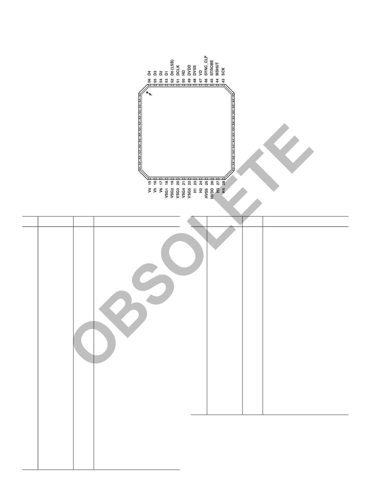
AD9995
PIN CONFIGURATION
D5 1
D6 2
PIN 1
IDENTIFIER
42 SDI
41 SL
D7 3
40 REFB
D8 4
39 REFT
D9 5
38 AVSS
D10 6
37 CCDIN
(MSB) D11 7
AD9995
36 AVDD
TOP VIEW
Pin
1
2
3
4
5
6
7
8
9
10
11
12
13
14
15
16
17
18
19
20
21
Mnemonic
D5
D6
D7
D8
D9
D10
D11
DRVDD
DRVSS
VSUB
SUBCK
V1
V2
V3
V4
V5
V6
VSG1
VSG2
VSG3
VSG4
DRVDD 8
DRVSS 9
VSUB 10
SUBCK 11
V1 12
V2 13
V3 14
35 CLI
34 CLO
33 TCVDD
32 TCVSS
31 RGVDD
30 RG
29 RGVSS
TE Type2
E DO
DO
DO
L DO
DO
DO
DO
P
O P
DO
DO
DO
S DO
DO
DO
DO
B DO
DO
DO
DO
ODO
PIN FUNCTION DESCRIPTIONS1
Description
Pin Mnemonic
Data Output
36 AVDD
Data Output
37 CCDIN
Data Output
38 AVSS
Data Output
39 REFT
Data Output
40 REFB
Data Output
41 SL
Data Output (MSB)
42 SDI
Data Output Driver Supply
43 SCK
Data Output Driver Ground
44 MSHUT
CCD Substrate Bias
45 STROBE
CCD Substrate Clock (E-Shutter) 46 SYNC
CCD Vertical Transfer Clock 1
47 VD
CCD Vertical Transfer Clock 2
CCD Vertical Transfer Clock 3
CCD Vertical Transfer Clock 4
48 DVSS
CCD Vertical Transfer Clock 5
49 DVDD
CCD Vertical Transfer Clock 6
CCD Sensor Gate Pulse 1
CCD Sensor Gate Pulse 2
50 HD
CCD Sensor Gate Pulse 3
CCD Sensor Gate Pulse 4
Type2
P
AI
P
AO
AO
DI
DI
DI
DO
DO
DI
DIO
P
P
DIO
Description
Analog Supply for AFE
CCD Signal Input
Analog Ground for AFE
Voltage Reference Top Bypass
Voltage Reference Bottom Bypass
3-Wire Serial Load Pulse
3-Wire Serial Data Input
3-Wire Serial Clock
Mechanical Shutter Pulse
Strobe Pulse
External System Sync Input
Vertical Sync Pulse
(Input for Slave Mode,
Output for Master Mode)
Digital Ground
Power Supply for VSG, V1–V6,
HD/VD, MSHUT, STROBE,
SYNC, and Serial Interface
Horizontal Sync Pulse
(Input for Slave Mode, Output for
Master Mode)
22 VSG5
DO CCD Sensor Gate Pulse 5
51 DCLK
DO Data Clock Output
23 H1
DO CCD Horizontal Clock 1
52 D0
DO Data Output (LSB)
24 H2
DO CCD Horizontal Clock 2
53 D1
DO Data Output
25 HVSS
P
H1–H4 Driver Ground
54 D2
DO Data Output
26 HVDD
P
H1–H4 Driver Supply
55 D3
DO Data Output
27 H3
DO CCD Horizontal Clock 3
56 D4
DO Data Output
28 H4
29 RGVSS
30 RG
31 RGVDD
DO CCD Horizontal Clock 4
P
RG Driver Ground
DO CCD Reset Gate Clock
P
RG Driver Supply
NOTES
1See Figure 38 for circuit configuration.
2AI = Analog Input, AO = Analog Output, DI = Digital Input,
DO = Digital Output, DIO = Digital Input/Output, P = Power.
32 TCVSS
P
Analog Ground for Timing Core
33 TCVDD P
Analog Supply for Timing Core
34 CLO
DO Clock Output for Crystal
35 CLI
DI Reference Clock Input
–6–
REV. 0
Share Link: 