AD9995KCP データシートの表示(PDF) - Analog Devices
部品番号
コンポーネント説明
メーカー
AD9995KCP Datasheet PDF : 60 Pages
| |||
AD9995
SYSTEM OVERVIEW
The H-drivers for H1–H4 and RG are included in the AD9995,
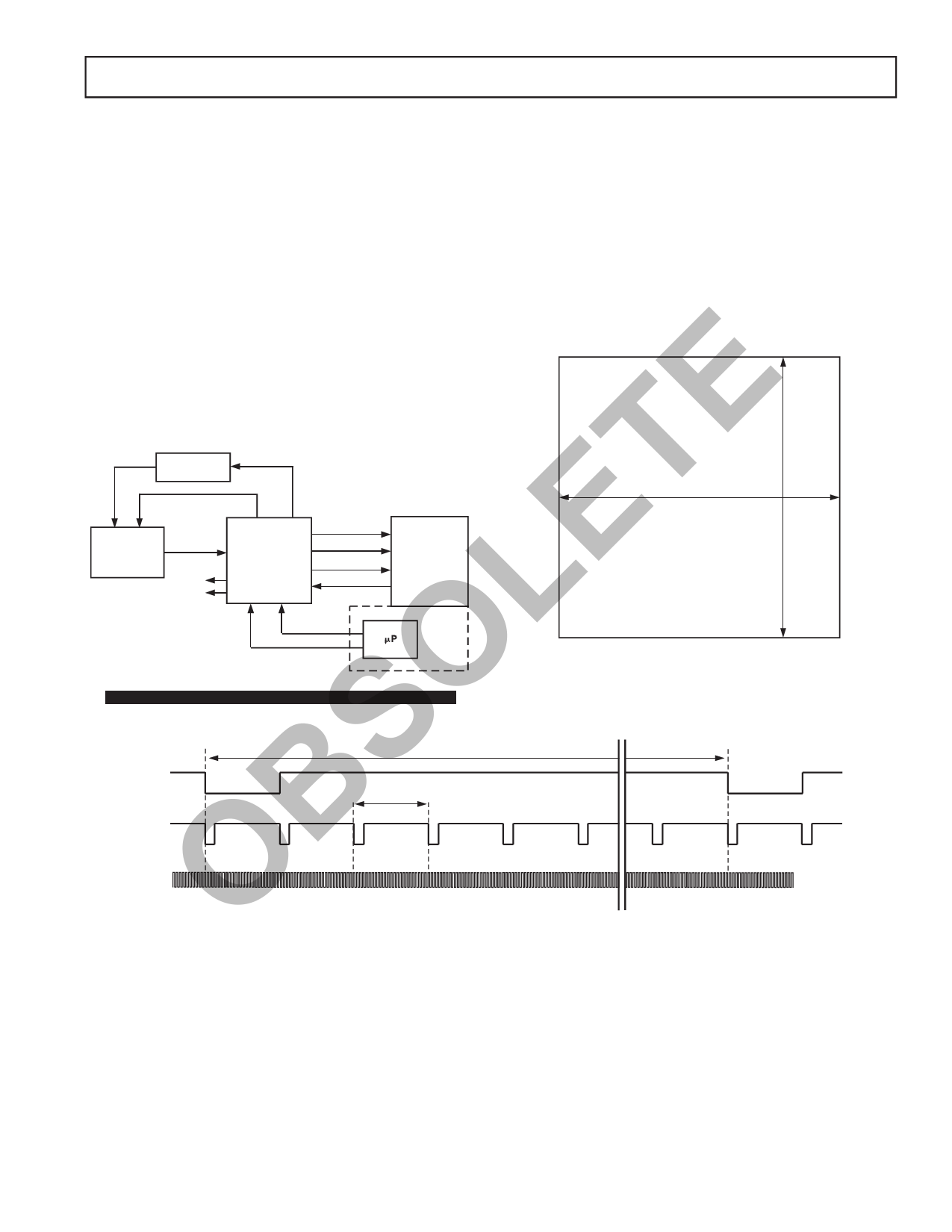
Figure 1 shows the typical system block diagram for the AD9995 allowing these clocks to be directly connected to the CCD.
used in Master mode. The CCD output is processed by the
H-drive voltage of up to 3.3 V is supported. An external V-driver
AD9995’s AFE circuitry, which consists of a CDS, VGA, black
is required for the vertical transfer clocks, the sensor gate pulses,
level clamp, and A/D converter. The digitized pixel information
and the substrate clock.
is sent to the digital image processor chip, which performs the
postprocessing and compression. To operate the CCD, all CCD
The AD9995 also includes programmable MSHUT and
STROBE outputs, which may be used to trigger mechanical
timing parameters are programmed into the AD9995 from the
shutter and strobe (flash) circuitry.
system microprocessor through the 3-wire serial interface. From
the system master clock, CLI, provided by the image processor
Figures 2 and 3 show the maximum horizontal and vertical
or external crystal, the AD9995 generates all of the CCD’s hori-
counter dimensions for the AD9995. All internal horizontal and
zontal and vertical clocks and all internal AFE clocks. External
vertical clocking is controlled by these counters to specify line
synchronization is provided by a SYNC pulse from the micropro- and pixel locations. Maximum HD length is 4095 pixels per line,
cessor, which will reset internal counters and resync the VD and
HD outputs.
Alternatively, the AD9995 may be operated in Slave mode, in
which VD and HD are provided externally from the image pro-
cessor. In this mode, all AD9995 timing will be synchronized
E with VD and HD.
V-DRIVER
V1–V6, VSG1–VSG5, SUBCK
LET CCD
H1–H4, RG, VSUB
CCDIN
MSHUT
STROBE
AD9995
AFETG
DOUT
DCLK
HD, VD
CLI
SYNC
SERIAL
INTERFACE
DIGITAL
IMAGE
PROCESSING
ASIC
Figure 1. Typical System Block Diagram, Master Mode
and maximum VD length is 4095 lines per field.
MAXIMUM
FIELD
DIMENSIONS
12-BIT HORIZONTAL = 4096 PIXELS MAX
12-BIT VERTICAL = 4096 LINES MAX
Figure 2. Vertical and Horizontal Counters
O MAX VD LENGTH IS 4095 LINES
S VD
MAX HD LENGTH IS 4095 PIXELS
HD
OB CLI
Figure 3. Maximum VD/HD Dimensions
REV. 0
–9–
Share Link: 