ADG1404YRUZ(RevB) гГЗгГЉгВњгВЈгГЉгГИгБЃи°®з§ЇпЉИPDFпЉЙ - Analog Devices
йГ®еУБзХ™еПЈ
гВ≥гГ≥гГЭгГЉгГНгГ≥гГИи™ђжШО
гГ°гГЉгВЂгГЉ
ADG1404YRUZ Datasheet PDF : 16 Pages
| |||
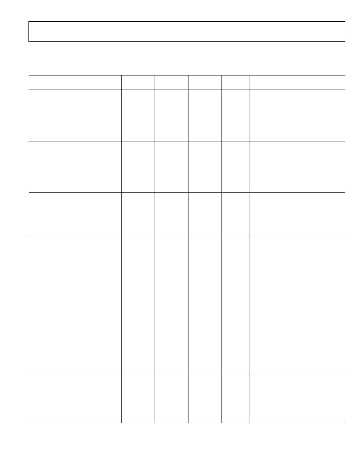
Data Sheet
ADG1404
5 V DUAL SUPPLY
VDD = 5 V ¬± 10%, VSS = вИТ5 V ¬± 10%, GND = 0 V, unless otherwise noted.
Table 3.
Parameter
ANALOG SWITCH
Analog Signal Range
On Resistance (RON)
On-Resistance Match
Between Channels (вИЖRON)
On-Resistance Flatness (RFLAT(ON))
LEAKAGE CURRENTS
Source Off Leakage, IS (Off)
Drain Off Leakage, ID (Off)
Channel On Leakage, ID, IS (On)
DIGITAL INPUTS
Input High Voltage, VINH
Input Low Voltage, VINL
Input Current, IINL or IINH
25¬∞C вИТ40¬∞C to +85¬∞C
3.3
4
4.9
0.13
0.22 0.23
0.9
1.1 1.24
±0.02
±0.2 ±1
±0.02
±0.25 ±1.2
±0.05
±0.25 ±1.5
0.001
Digital Input Capacitance, CIN
35
DYNAMIC CHARACTERISTICS1
Transition Time, tTRANSITION
340
470 560
tON (EN)
260
355 430
tOFF (EN)
220
315 365
Break-Before-Make Time Delay, tBBM 100
Charge Injection
30
Off Isolation
80
вИТ40¬∞C to +125¬∞C
VDD to VSS
5.4
0.25
1.31
±12.5
±15
±20
2.0
0.8
±0.1
615
480
400
50
Channel-to-Channel Crosstalk
82
вИТ3 dB Bandwidth
40
Insertion Loss
0.27
Total Harmonic Distortion + Noise
0.03
CS (Off)
CD (Off)
CD, CS (On)
POWER REQUIREMENTS
IDD
33
128
210
0.001
ISS
0.001
VDD/VSS
1 Guaranteed by design, not subject to production test.
1
1
±4.5/±16.5
Unit
V
вД¶ typ
вД¶ max
вД¶ typ
вД¶ max
вД¶ typ
вД¶ max
nA typ
nA max
nA typ
nA max
nA typ
nA max
V min
V max
µA typ
µA max
pF typ
ns typ
ns max
ns typ
ns max
ns typ
ns max
ns typ
ns min
pC typ
dB typ
dB typ
MHz typ
dB typ
% typ
pF typ
pF typ
pF typ
µA typ
µA max
µA typ
µA max
V min/max
Test Conditions/Comments
VS = ¬±4.5 V, IS = вИТ10 mA; see Figure 22
VDD = +4.5 V, VSS = вИТ4.5 V
VS = ¬±4.5 V, IS = вИТ10 mA
VS = ¬±4.5 V, IS = вИТ10 mA
VDD = +5.5 V, VSS = вИТ5.5 V
VS = ¬±4.5 V, VD = вИУ4.5 V; see Figure 23
VS = ¬±4.5 V, VD = вИУ4.5 V; see Figure 23
VS = VD = ±4.5 V; see Figure 24
VIN = VGND or VDD
RL = 300 вД¶, CL = 35 pF
VS = 3 V; Figure 29
RL = 300 вД¶, CL = 35 pF
VS = 3 V; Figure 31
RL = 300 вД¶, CL = 35 pF
VS = 3 V; Figure 31
RL = 300 вД¶, CL = 35 pF
VS1 = VS2 = 3 V; see Figure 30
VS = 0 V, RS = 0 вД¶, CL = 1 nF; see Figure 32
RL = 50 вД¶, CL = 5 pF, f = 100 kHz;
see Figure 25
RL = 50 вД¶, CL = 5 pF, f = 100 kHz;
see Figure 27
RL = 50 вД¶, CL = 5 pF; see Figure 26
RL = 50 вД¶, CL = 5 pF, f = 1 MHz; see Figure 26
RL = 110 вД¶, 2.5 V p-p, f = 20 Hz to 20 kHz;
see Figure 28
VS = 0 V, f = 1 MHz
VS = 0 V, f = 1 MHz
VS = 0 V, f = 1 MHz
VDD = 5.5 V, VSS = вИТ5.5 V
Digital inputs = 0 V, 5 V, or VDD
Digital inputs = 0 V or VDD
GND = 0 V
Rev. B | Page 5 of 16
Share Link: 