ADG1406BRUZ-REEL7 гГЗгГЉгВњгВЈгГЉгГИгБЃи°®з§ЇпЉИPDFпЉЙ - Analog Devices
йГ®еУБзХ™еПЈ
гВ≥гГ≥гГЭгГЉгГНгГ≥гГИи™ђжШО
гГ°гГЉгВЂгГЉ
ADG1406BRUZ-REEL7
Analog Devices

ADG1406BRUZ-REEL7 Datasheet PDF : 20 Pages
| |||
ADG1406/ADG1407
Parameter
CD, CS (On)
ADG1406
ADG1407
POWER REQUIREMENTS
IDD
+25°C
115
70
0.002
IDD
280
ISS
0.002
VDD/VSS
1 Temperature range for B version is вИТ40¬∞C to +125¬∞C.
2 Guaranteed by design, not subject to production test.
вИТ40¬∞C to вИТ40¬∞C to
+85°C +125°C1
Unit
Test Conditions/Comments
1
400
1
±4.5/±16.5
pF typ
pF typ
ќЉA typ
ќЉA max
ќЉA typ
ќЉA max
ќЉA typ
ќЉA max
V min/max
f = 1 MHz
f = 1 MHz
VDD = +16.5 V, VSS = вИТ16.5 V
Digital inputs = 0 V or VDD
Digital inputs = 5 V
Digital inputs = 0 V, 5 V or VDD
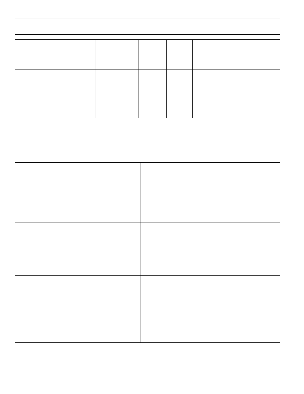
12 V SINGLE SUPPLY
VDD = 12 V ± 10%, VSS = 0 V, GND = 0 V, unless otherwise noted.
Table 3.
Parameter
ANALOG SWITCH
Analog Signal Range
On Resistance (RON)
On-Resistance Match Between
Channels (ќФRON)
On-Resistance Flatness (RFLAT(ON))
LEAKAGE CURRENTS
Source Off Leakage, IS (Off )
вИТ40¬∞C to
+25°C +85°C
18
21.5 26
0.55
1.2
1.6
5
6
6.9
±0.01
вИТ40¬∞C to
+125°C1
0 to VDD
28.5
1.8
7.3
±0.25 ±1
±4
Drain Off Leakage, ID (Off )
±0.01
±0.5 ±3
±20
Channel On Leakage, ID, IS (On)
±0.01
±0.5 ±3
±20
DIGITAL INPUTS
Input High Voltage, VINH
2.0
Input Low Voltage, VINL
0.8
Input Current
±0.002
±0.1
Digital Input Capacitance, CIN
4
DYNAMIC CHARACTERISTICS2
Transition Time, tTRANSITION
170
250 310
350
Break-Before-Make Time Delay, tBBM 75
30
Unit
V
ќ© typ
ќ© max
ќ© typ
ќ© max
ќ© typ
ќ© max
nA typ
nA max
nA typ
nA max
nA typ
nA max
V min
V max
ќЉA typ
ќЉA max
pF typ
ns typ
ns max
ns typ
ns min
Test Conditions/Comments
VDD = 10.8 V, VSS = 0 V; VS = 0 V to 10 V,
IS = вИТ10 mA; see Figure 27
VDD = 10.8 V, VSS = 0 V; VS = 0 V to 10 V,
IS = вИТ10 mA
VDD = 10.8 V, VSS = 0 V; VS = 0 V to 10 V,
IS = вИТ10 mA
VDD = 10.8 V
VS = 1 V/10 V, VD = 10 V/1 V; see
Figure 28
VS = 1 V/10 V, VD = 10 V/1 V; see
Figure 28
VS = VD = 1 V or 10 V; see Figure 29
VIN = VGND or VDD
RL = 100 ќ©, CL = 35 pF
VS = 8 V; see Figure 29
RL = 100 ќ©, CL = 35 pF
VS1 = VS2 = 8 V; see Figure 31
Rev. 0 | Page 4 of 20
Share Link: