ADIS16227 データシートの表示(PDF) - Analog Devices
部品番号
コンポーネント説明
メーカー
ADIS16227 Datasheet PDF : 24 Pages
| |||
Data Sheet
ADIS16227
THEORY OF OPERATION
The ADIS16227 is a triaxial, wide bandwidth, vibration-sensing
system. It combines a triaxial MEMS accelerometer with a
sampling and advanced signal processing system. The SPI-
compatible port and user register structure provide convenient
access to frequency domain vibration data and many user
controls.
SENSING ELEMENT
TRIAXIAL
MEMS
SENSOR
TEMP
SENSOR
ADC
CAPTURE
BUFFER
OUTPUT
REGISTERS
CONTROLLER
CONTROL
REGISTERS
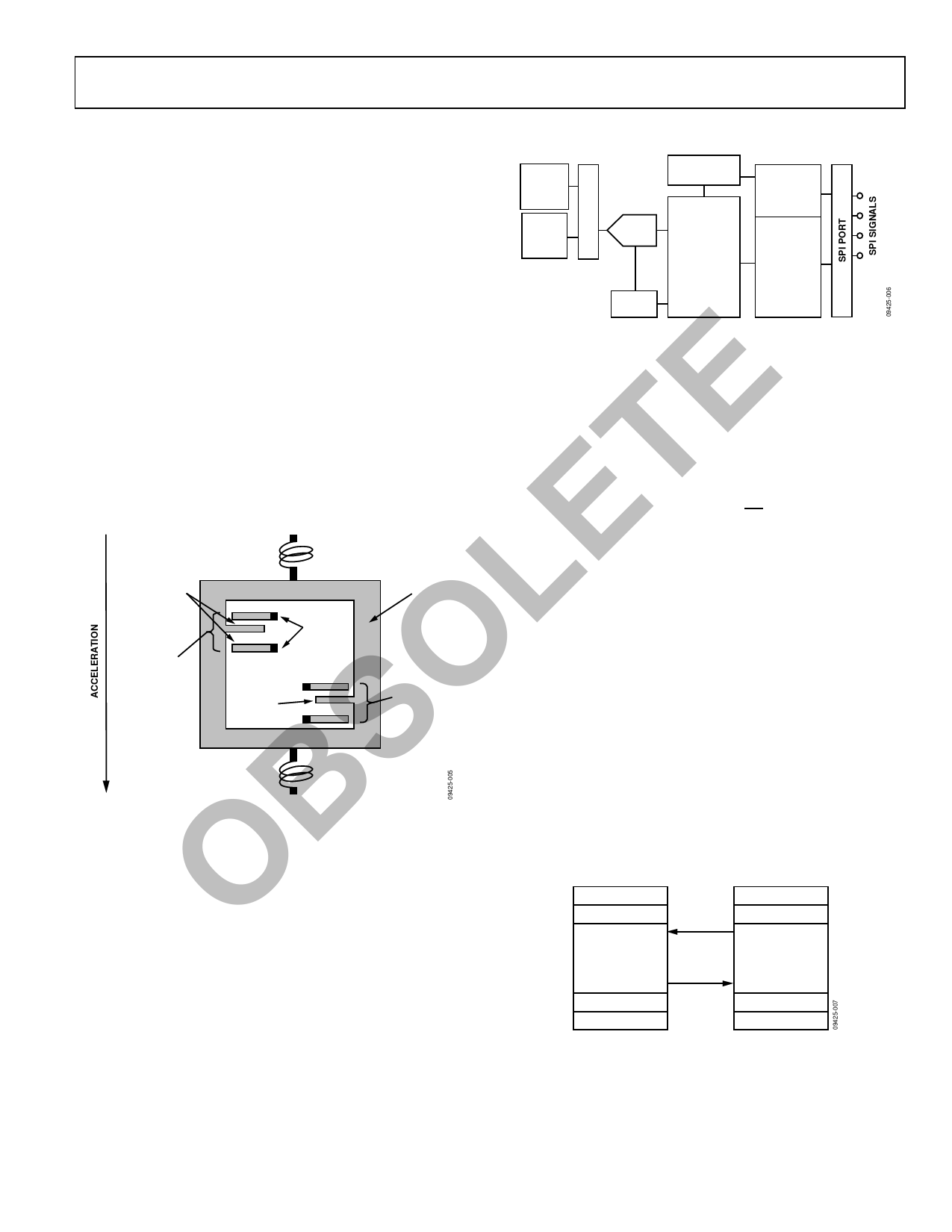
Digital vibration sensing in the ADIS16227 starts with a wide
CLOCK
bandwidth MEMS accelerometer core on each axis, which provides
Figure 6. Simplified Sensor Signal Processing Diagram
a linear motion-to-electrical transducer function. Figure 5 provides
a basic physical diagram of the sensing element and its response
to linear acceleration. It uses a fixed frame and a moving frame
to form a differential capacitance network that responds to linear
acceleration. Tiny springs tether the moving frame to the fixed
E frame and govern the relationship between acceleration and
physical displacement. A modulation signal on the moving plate
feeds through each capacitive path into the fixed frame plates and
T into a demodulation circuit, which produces the electrical signal
that is proportional to the acceleration acting on the device.
ANCHOR
E PLATE
CAPACITORS
MOVABLE
FRAME
L UNIT SENSING
O CELL
FIXED
PLATES
MOVING
PLATE
UNIT
FORCING
CELL
S ANCHOR
Figure 5. MEMS Sensor Diagram
B SIGNAL PROCESSING
Figure 6 offers a simplified block diagram for the ADIS16227.
The signal processing stage includes time domain data capture,
O digital decimation/filtering, windowing, FFT analysis, FFT
USER INTERFACE
SPI Interface
The user registers manage user access to both sensor data and
configuration inputs. Each 16-bit register has its own unique bit
assignment and two addresses: one for its upper byte and one for
its lower byte. Table 8 provides a memory map for each register,
along with its function and lower byte address. The data
collection and configuration command uses the SPI, which
consists of four wires. The chip select (CS) signal activates the
SPI interface, and the serial clock (SCLK) synchronizes the
serial data lines. Input commands clock into the DIN pin, one
bit at a time, on the SCLK rising edge. Output data clocks out of
the DOUT pin on the SCLK falling edge. When the SPI is used
as a slave device, the DOUT contents reflect the information
requested using a DIN command.
Dual Memory Structure
The user registers provide addressing for all input/output operations
in the SPI interface. The control registers use a dual memory
structure. The controller uses SRAM registers for normal
operation, including user-configuration commands. The flash
memory provides nonvolatile storage for control registers that
have flash backup (see Table 8). Storing configuration data in
the flash memory requires a manual flash update command
(GLOB_CMD[6] = 1, DIN = 0xBE40). When the device powers
on or resets, the flash memory contents load into the SRAM, and
the device starts producing data according to the configuration
in the control registers.
MANUAL
FLASH
averaging, and record storage. See Figure 13 for more details on
BACKUP
the signal processing operation.
NONVOLATILE
FLASH MEMORY
(NO SPI ACCESS)
VOLATILE
SRAM
SPI ACCESS
START-UP
RESET
Figure 7. SRAM and Flash Memory Diagram
Rev. B | Page 7 of 24
Share Link: 