ADL5354(RevA) データシートの表示(PDF) - Analog Devices
部品番号
コンポーネント説明
メーカー
ADL5354
(Rev.:RevA)
(Rev.:RevA)
Analog Devices

ADL5354 Datasheet PDF : 24 Pages
| |||
ADL5354
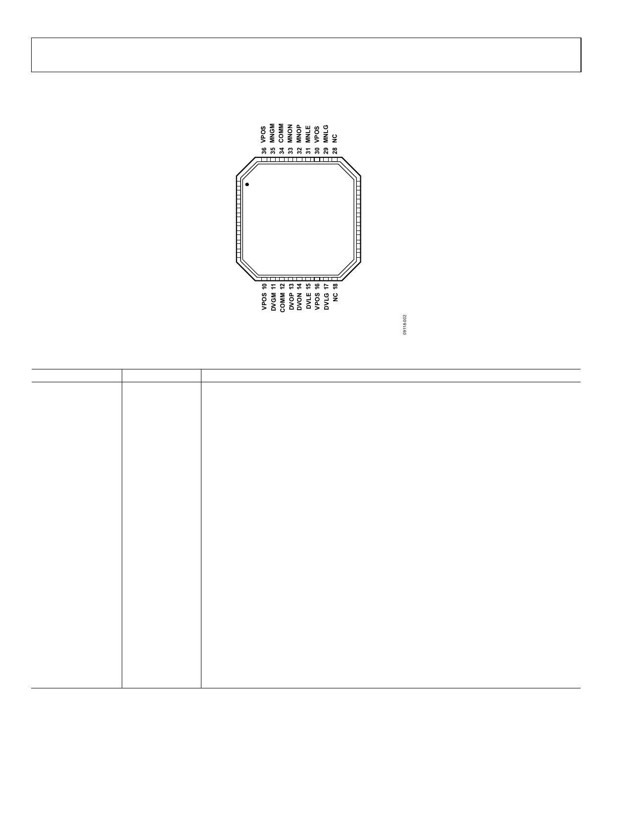
PIN CONFIGURATION AND FUNCTION DESCRIPTIONS
Data Sheet
MNIN 1
MNCT 2
COMM 3
VPOS 4
COMM 5
VPOS 6
COMM 7
DVCT 8
DVIN 9
ADL5354
TOP VIEW
(Not to Scale)
27 LOI2
26 VGS2
25 VGS1
24 VGS0
23 LOSW
22 PWDN
21 VPOS
20 COMM
19 LOI1
Table 6. Pin Function Descriptions
Pin No.
Mnemonic
1
MNIN
2
MNCT
3, 5, 7, 12, 20, 34
COMM
4, 6, 10, 16, 21, 30, 36 VPOS
8
DVCT
9
DVIN
11
DVGM
13, 14
DVOP, DVON
15
17
18, 28
19
22
DVLE
DVLG
NIC
LOI1
PWDN
23
24, 25, 26
27
29
31
32, 33
LOSW
VGS0, VGS1,
VGS2
LOI2
MNLG
MNLE
MNOP, MNON
35
MNGM
EPAD
NOTES
1. NIC = NO INTERNAL CONNECTION.
2. THE EXPOSED PAD MUST BE CONNECTED TO GROUND.
Figure 2. Pin Configuration
Description
RF Input for Main Channel. Internally matched to 50 Ω. Must be ac-coupled.
Center Tap for Main Channel Input Balun. Bypass to ground using low inductance capacitor.
Device Common (DC Ground).
Positive Supply Voltage.
Center Tap for Diversity Channel Input Balun. Bypass to ground using low inductance capacitor.
RF Input for Diversity Channel. Internally matched to 50 Ω. Must be ac-coupled.
Diversity Amplifier Bias Setting. Connect a 1.3 kΩ resistor to ground for typical operation.
Diversity Channel Differential Open-Collector Outputs. DVOP and DVON should be pulled up to
VCC using external inductors, see Figure 53 for details.
Diversity Channel IF Return. This pin must be grounded.
Diversity Channel LO Buffer Bias Setting. Connect a 1 kΩ resistor to ground for typical operation.
No Internal Connection. Do not connect to this pin.
Local Oscillator Input 1. Internally matched to 50 Ω. Must be ac-coupled.
Power Down. Connect this pin to ground for normal operation. Connect pin to 3 V for disable
mode when using VPOS ≤ 3.6 V. PWDN pin must be grounded when VPOS > 3.6 V.
Local Oscillator Input Selection Switch. Set LOSW high to select LOI1 or set LOSW low to select LOI2.
Gate to Source Control Voltages. For typical operation, set VGS0, VGS1, and VGS2 to a low logic
level.
Local Oscillator Input 2. Internally matched to 50 Ω. Must be ac-coupled.
Main Channel LO Buffer Bias Setting. Connect a 1 kΩ resistor to ground for typical operation.
Main Channel IF Return. This pin must be grounded.
Main Channel Differential Open-Collector Outputs. Pull up MNOP and MNON to VCC by using
external inductors, see Figure 53 for details.
Main Amplifier Bias Setting. Connect a 1.3 kΩ resistor to ground for typical operation.
Exposed Pad. The exposed pad must be connected to ground.
Rev. A | Page 6 of 24
Share Link: