ADM1168 データシートの表示(PDF) - Analog Devices
部品番号
コンポーネント説明
メーカー
ADM1168 Datasheet PDF : 27 Pages
| |||
Data Sheet
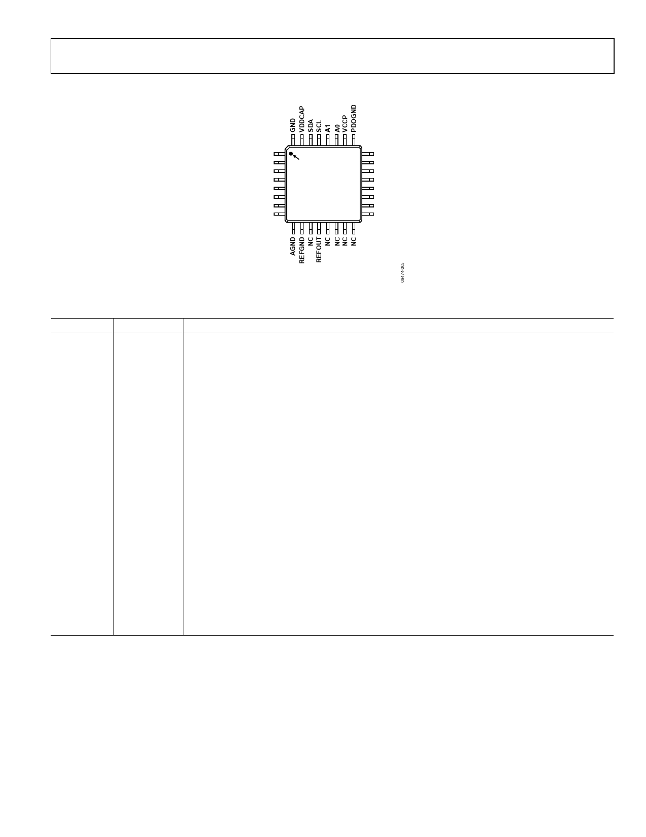
PIN CONFIGURATION AND FUNCTION DESCRIPTIONS
ADM1168
32
VX1 1
VX2
VX3
VX4
VP1
VP2
VP3
VH 8
9
PIN 1
INDICATOR
ADM1168
TOP VIEW
(Not to Scale)
25
24 PDO1
PDO2
PDO3
PDO4
PDO5
PDO6
PDO7
17 PDO8
16
NC = NO CONNECT.
DO NOT CONNECT TO THIS PIN.
Figure 3. Pin Configuration
Table 4. Pin Function Descriptions
Pin No.
Mnemonic
Description
1 to 4
VX1 to VX4
High Impedance Inputs to Supply Fault Detectors. Fault thresholds can be set from 0.573 V to 1.375 V.
Alternatively, these pins can be used as general-purpose digital inputs.
5 to 7
VP1 to VP3
Low Voltage Inputs to Supply Fault Detectors. Three input ranges can be set by altering the input attenuation
on a potential divider connected to these pins, the output of which connects to a supply fault detector.
These pins allow thresholds from 2.5 V to 6 V, from 1.25 V to 3 V, and from 0.573 V to 1.375 V.
8
VH
High Voltage Input to Supply Fault Detectors. Three input ranges can be set by altering the input attenuation
on a potential divider connected to this pin, the output of which connects to a supply fault detector.
This pin allows thresholds from 6 V to 14.4 V and from 2.5 V to 6 V.
9
AGND1
Ground Return for Input Attenuators.
10
REFGND1
Ground Return for On-Chip Reference Circuits.
11, 13 to 16 NC
No Connect. Do not connect to this pin.
12
REFOUT
Reference Output, 2.048 V. Note that a capacitor must always be connected between this pin and REFGND.
A 10 μF capacitor is recommended for this purpose.
17 to 24
PDO8 to PDO1 Programmable Output Drivers.
25
PDOGND1
Ground Return for Output Drivers.
26
VCCP
Central Charge-Pump Voltage of 5.25 V. A reservoir capacitor must be connected between this pin and
GND. A 10 μF capacitor is recommended for this purpose.
27
A0
Logic Input. This pin sets the seventh bit of the SMBus interface address.
28
A1
Logic Input. This pin sets the sixth bit of the SMBus interface address.
29
SCL
SMBus Clock Pin. Bidirectional open drain requires external resistive pull-up.
30
SDA
SMBus Data Pin. Bidirectional open drain requires external resistive pull-up.
31
VDDCAP
Device Supply Voltage. Linearly regulated from the highest of the VPx and VH pins to a typical of 4.75 V.
A capacitor must be connected between this pin and GND. A 10 μF capacitor is recommended for
this purpose.
32
GND1
Supply Ground.
1 In a typical application, all ground pins are connected together.
Rev. B | Page 7 of 27
Share Link: 