ADN2811(RevA) データシートの表示(PDF) - Analog Devices
部品番号
コンポーネント説明
メーカー
ADN2811
(Rev.:RevA)
(Rev.:RevA)
Analog Devices

ADN2811 Datasheet PDF : 16 Pages
| |||
ADN2811
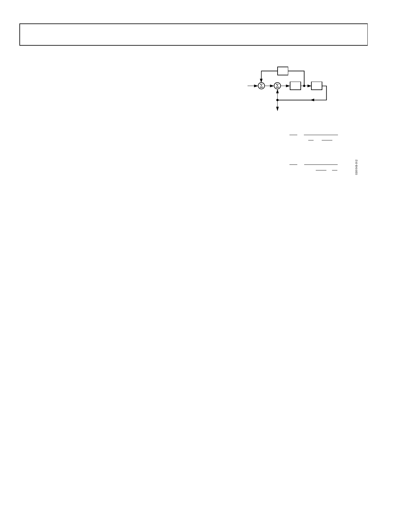
FUNCTIONAL DESCRIPTION
Clock and Data Recovery
The ADN2811 will recover clock and data from serial bit streams
at OC-48 as well as the 15/14 FEC rates. The data rate is selected
by the RATE input (see Table I).
Table I. Data Rate Selection
RATE
0
1
Data Rate
OC-48
OC-48 FEC
Frequency (MHz)
2488.32
2666.06
Limiting Amplifier
The limiting amplifier has differential inputs (PIN/NIN) that are
internally terminated with 50 Ω to an on-chip voltage reference
(VREF = 0.6 V typically). These inputs are normally ac-coupled,
although dc-coupling is possible as long as the input common-mode
voltage remains above 0.4 V (see Figures 20–22). Input offset is
factory trimmed to achieve better than 4 mV typical sensitivity
with minimal drift. The limiting amplifier can be driven
differentially or single-ended.
Slice Adjust
The quantizer slicing level can be offset by ± 100 mV to mitigate
the effect of ASE (amplified spontaneous emission) noise by
applying a differential voltage input of ± 0.8 V to SLICEP/N
inputs. If no adjustment of the slice level is needed, SLICEP/N
should be tied to VCC.
Loss of Signal (LOS) Detector
The receiver front end level signal detect circuit indicates when
the input signal level has fallen below a user adjustable threshold.
The threshold is set with a single external resistor from Pin 1,
THRADJ, to GND. The LOS comparator trip point versus the
resistor value is illustrated in Figure 2 (this is only valid for
SLICEP = SLICEN = VCC). If the input level to the ADN2811
drops below the programmed LOS threshold, SDOUT (Pin 45)
will indicate the loss of signal condition with a Logic 1. The LOS
response time is ~300 ns by design but will be dominated by the
RC time constant in ac-coupled applications.
If the LOS detector is used, the quantizer slice adjust pins must
both be tied to VCC. This is to avoid interaction with the LOS
threshold level.
Note that it is not expected to use both LOS and slice adjust at
the same time; systems with optical amplifiers need the slice
adjust to evade ASE. However, a loss of signal in an optical link
that uses optical amplifiers causes the optical amplifier output to
be full-scale noise. Under this condition, the LOS would not
detect the failure. In this case, the loss of lock signal will indi-
cate the failure because the CDR circuitry will not be able to
lock onto a signal that is full-scale noise.
Reference Clock
There are three options for providing the reference frequency to
the ADN2811: differential clock, single-ended clock, or crystal
oscillator. See Figures 12–14 for example configurations.
The ADN2811 can accept any of the following reference clock
frequencies: 19.44 MHz, 38.88 MHz, 77.76 MHz at LVTTL/
LVCMOS/LVPECL/LVDS levels or 155.52 MHz at LVPECL/
LVDS levels via the REFCLKN/P inputs, independent of data
rate. The input buffer accepts any differential signal with a
peak-to-peak differential amplitude of greater than 100 mV
(e.g., LVPECL or LVDS) or a standard single-ended low volt-
age TTL input, providing maximum system flexibility. The
appropriate division ratio can be selected using the REFSEL0/1
pins, according to Table II. Phase noise and duty cycle of the
reference clock are not critical and 100 ppm accuracy is sufficient.
ADN2811
REFCLKP
BUFFER
REFCLKN
VCC
VCC
XO1
XO2
100k⍀ 100k⍀
VCC/2
CRYSTAL
OSCILLATOR
VCC
REFSEL
Figure 12. Differential REFCLK Configuration
VCC
CLK
OSC OUT
REFCLKP
ADN2811
BUFFER
NC
REFCLKN
100k⍀ 100k⍀
VCC/2
VCC
VCC
XO1
XO2
CRYSTAL
OSCILLATOR
VCC
REFSEL
Figure 13. Single-Ended REFCLK Configuration
ADN2811
VCC
REFCLKP
NC
REFCLKN
19.44MHz
XO1
XO2
BUFFER
100k⍀ 100k⍀
VCC/2
CRYSTAL
OSCILLATOR
REFSEL
Figure 14. Crystal Oscillator Configuration
–10–
REV. A
Share Link: