ADN2811(RevA) データシートの表示(PDF) - Analog Devices
部品番号
コンポーネント説明
メーカー
ADN2811
(Rev.:RevA)
(Rev.:RevA)
Analog Devices

ADN2811 Datasheet PDF : 16 Pages
| |||
ADN2811
THEORY OF OPERATION
The ADN2811 is a delay-locked and phase-locked loop circuit
for clock recovery and data retiming from an NRZ encoded data
stream. The phase of the input data signal is tracked by two
separate feedback loops that share a common control voltage.
A high speed delay-locked loop path uses a voltage controlled
phase shifter to track the high frequency components of the
input jitter. A separate phase control loop, comprised of the
VCO, tracks the low frequency components of the input jitter.
The initial frequency of the VCO is set by yet a third loop, which
compares the VCO frequency with the reference frequency and
sets the coarse tuning voltage. The jitter tracking phase-locked
loop controls the VCO by the fine tuning control.
The delay-locked and phase-locked loops together track the
phase of the input data signal. For example, when the clock lags
input data, the phase detector drives the VCO to a higher
frequency and also increases the delay through the phase shifter.
Both of these actions both serve to reduce the phase error between
the clock and data. The faster clock picks up phase while the
delayed data loses phase. Since the loop filter is an integrator,
the static phase error will be driven to zero.
Another view of the circuit is that the phase shifter implements
the zero required for the frequency compensation of a second-
order phase-locked loop, and this zero is placed in the feedback
path and thus does not appear in the closed-loop transfer func-
tion. Jitter peaking in a conventional second-order phase-locked
loop is caused by the presence of this zero in the closed-loop
transfer function. Since this circuit has no zero in the closed-
loop transfer, jitter peaking is minimized.
The delay-locked and phase-locked loops together simultaneously
provide wideband jitter accommodation and narrow-band jitter
filtering. The linearized block diagram in Figure 10 shows the
jitter transfer function, Z(s)/X(s), is a second-order low-pass
providing excellent filtering. Note the jitter transfer has no zero,
unlike an ordinary second-order phase-locked loop. This means
that the main PLL loop has low jitter peaking (see Figure 11),
which makes this circuit ideal for signal regenerator applications
where jitter peaking in a cascade of regenerators can contribute
to hazardous jitter accumulation.
INPUT X(s)
DATA
psh
e(s)
d/sc
o/s
Z(s)
RECOVERED
CLOCK
d = PHASE DETECTOR GAIN
o = VCO GAIN
c = LOOP INTEGRATOR
psh = PHASE SHIFTER GAIN
n = DIVIDE RATIO
JITTER TRANSFER FUNCTION
Z(s)
X(s)
=
s2
cn
do
+
1
n
s
psh
o
+1
TRACKING ERROR TRANSFER FUNCTION
e(s) =
s2
X(s) s2 + s d psh + do
c cn
Figure 10. PLL/DLL Architecture
The error transfer, e(s)/X(s), has the same high-pass form as an
ordinary phase-locked loop. This transfer function is free to be
optimized to give excellent wideband jitter accommodation
since the jitter transfer function, Z(s)/X(s), provides the narrow-
band jitter filtering.
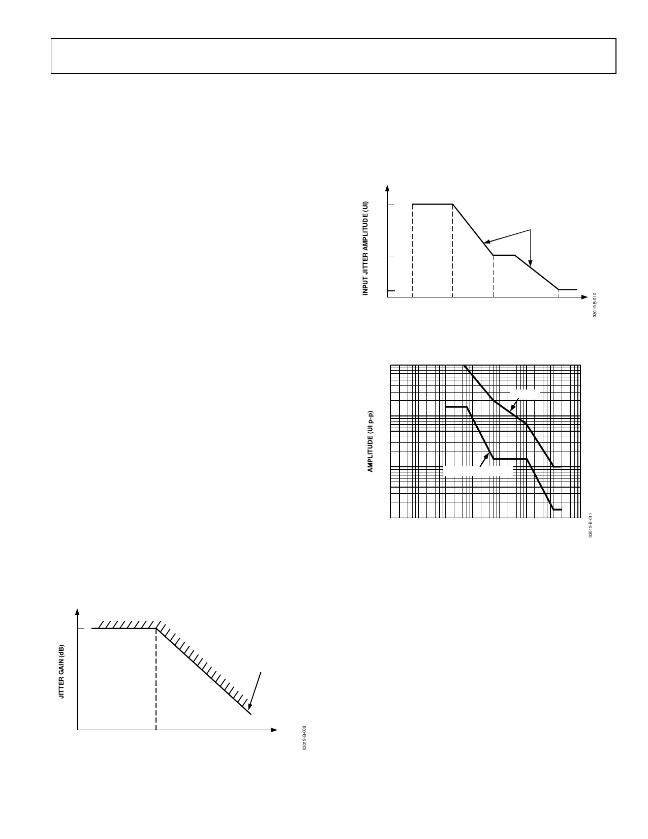
The delay-locked and phase-locked loops contribute to overall
jitter accommodation. At low frequencies of input jitter on the
data signal, the integrator in the loop filter provides high gain to
track large jitter amplitudes with small phase error. In this case,
the VCO is frequency modulated and jitter is tracked as in an
ordinary phase-locked loop. The amount of low frequency jitter
that can be tracked is a function of the VCO tuning range. A
wider tuning range gives larger accommodation of low fre-
quency jitter. The internal loop control voltage remains small
for small phase errors, so the phase shifter remains close to the
center of its range and thus contributes little to the low fre-
quency jitter accommodation.
At medium jitter frequencies, the gain and tuning range of the
VCO are not large enough to track the input jitter. In this case,
the VCO control voltage becomes large and saturates, and the
VCO frequency dwells at one or the other extreme of its tuning
range. The size of the VCO tuning range therefore has only a
small effect on the jitter accommodation. The delay-locked loop
control voltage is now larger, and so the phase shifter takes on
the burden of tracking the input jitter. The phase shifter range, in
UI, can be seen as a broad plateau on the jitter tolerance curve.
The phase shifter has a minimum range of 2 UI at all data rates.
The gain of the loop integrator is small for high jitter frequen-
cies, so larger phase differences are needed to make the loop
control voltage big enough to tune the range of the phase
shifter. Large phase errors at high jitter frequencies cannot be
tolerated. In this region, the gain of the integrator determines
the jitter accommodation. Since the gain of the loop integrator
declines linearly with frequency, jitter accommodation is lower
with higher jitter frequency. At the highest frequencies, the loop
gain is very small and little tuning of the phase shifter can be
expected. In this case, jitter accommodation is determined by
the eye opening of the input data, the static phase error, and the
residual loop jitter generation. The jitter accommodation is
roughly 0.5 UI in this region. The corner frequency between the
declining slope and the flat region is the closed loop bandwidth
of the delay-locked loop, which is roughly 5 MHz.
JITTER PEAKING
IN ORDINARY PLL
JITTER
GAIN
(dB)
ADN2811
Z(s)
X(s)
o
n psh
d psh
c
f (kHz)
Figure 11. Jitter Response vs. Conventional PLL
REV. A
–9–
Share Link: