ADN2811 データシートの表示(PDF) - Analog Devices
部品番号
コンポーネント説明
メーカー
ADN2811 Datasheet PDF : 20 Pages
| |||
LOS RESPONSE TIME
The LOS response time is the delay between the removal of the
input signal and the indication of loss of signal (LOS) at
SDOUT. The LOS response time of the ADN2811 is 300 ns typ
when the inputs are dc-coupled. In practice, the time constant
of the ac-coupling at the quantizer input determines the LOS
response time.
JITTER SPECIFICATIONS
The ADN2811 CDR is designed to achieve the best bit-error-
rate (BER) performance, and has exceeded the jitter generation,
transfer, and tolerance specifications proposed for SONET/SDH
equipment defined in the Telcordia Technologies specification.
Jitter is the dynamic displacement of digital signal edges from
their long-term average positions measured in UI (unit
intervals), where 1 UI = 1 bit period. Jitter on the input data
can cause dynamic phase errors on the recovered clock
sampling edge. Jitter on the recovered clock causes jitter on the
retimed data.
The following sections briefly summarize the specifications of
jitter generation, transfer, and tolerance in accordance with the
Telcordia document (GR-253-CORE, Issue 3, September 2000)
for the optical interface at the equipment level and the
ADN2811 performance with respect to those specifications.
Jitter Generation
Jitter generation specification limits the amount of jitter that
can be generated by the device with no jitter and wander
applied at the input. For OC-48 devices, the band-pass filter has
a 12 kHz high-pass cutoff frequency with a roll-off of
20 dB/decade and a low-pass cutoff frequency of at least
20 MHz. The jitter generated should be less than 0.01 UI rms
and 0.1 UI p-p.
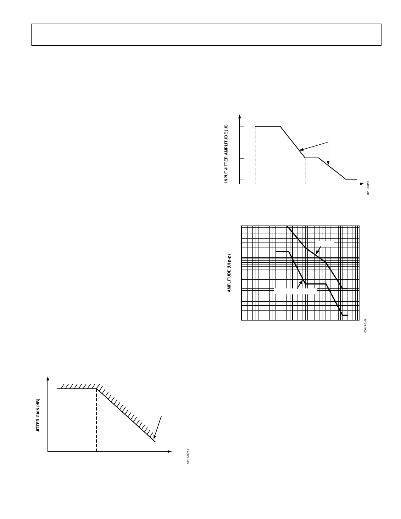
Jitter Transfer
Jitter transfer function is the ratio of the jitter on the output
signal to the jitter applied on the input signal versus the
frequency. This parameter measures the limited amount of jitter
on an input signal that can be transferred to the output signal
(see Figure 9).
0.1
ACCEPTABLE
RANGE
SLOPE = –20dB/DECADE
ADN2811
Jitter Tolerance
Jitter tolerance is defined as the peak-to-peak amplitude of the
sinusoidal jitter applied on the input signal that causes a 1 dB
power penalty. This is a stress test that is intended to ensure no
additional penalty is incurred under the operating conditions
(see Figure 10). Figure 11 shows the typical OC-48 jitter
tolerance performance of the ADN2811.
15
SLOPE = –20dB/DECADE
1.5
0.15
f0
f1
f2 f3
f4
JITTER FREQUENCY (Hz)
Figure 10. SONET Jitter Tolerance Mask
100
ADN2811
10
1
OC-48 SONET MASK
ٛ0.1
1
10
100
1k
10k 100k
1M
10M
MODULATION FREQUENCY (Hz)
Figure 11. OC-48 Jitter Tolerance Curve
fC
JITTER FREQUENCY (kHz)
Figure 9. Jitter Transfer Curve
Rev. B | Page 9 of 20
Share Link: 