ADN2820 データシートの表示(PDF) - Analog Devices
部品番号
コンポーネント説明
メーカー
ADN2820 Datasheet PDF : 12 Pages
| |||
ADN2820
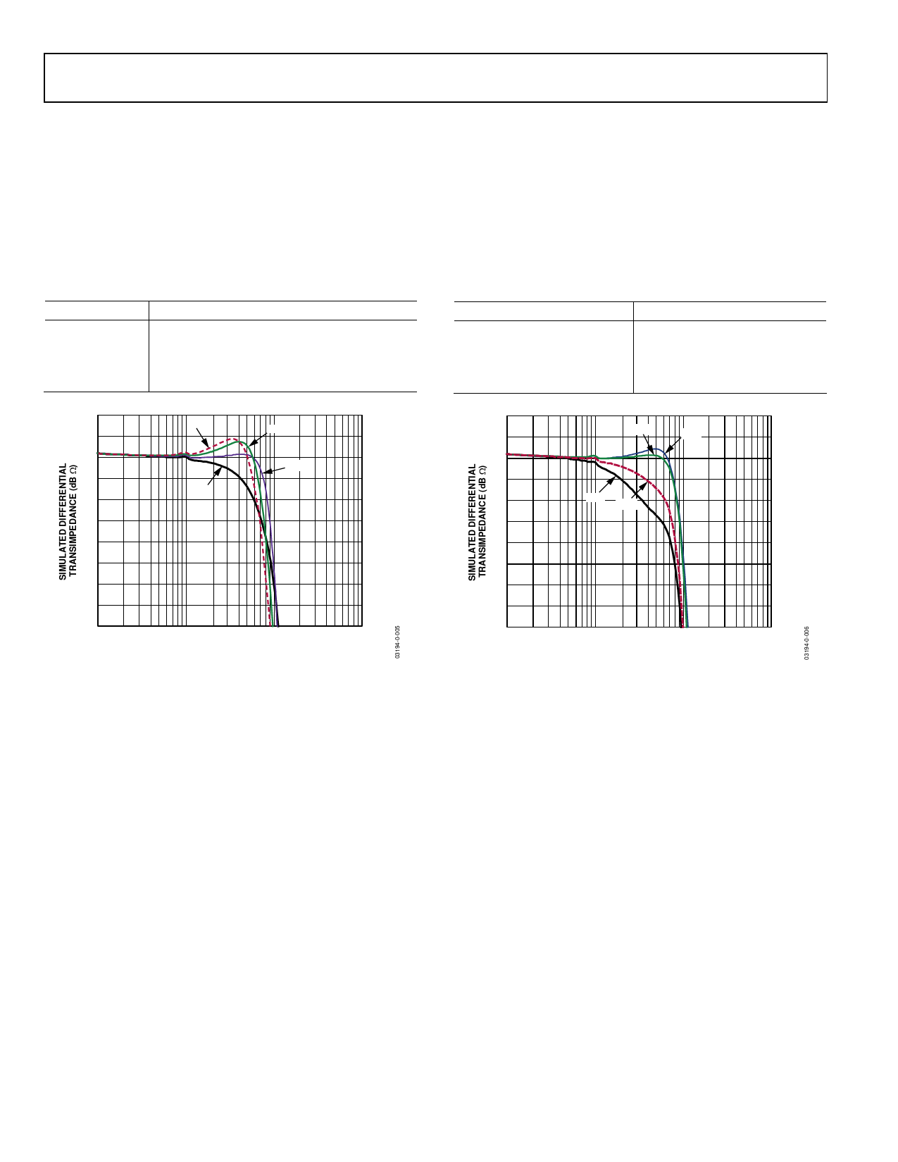
BANDWIDTH VERSUS INPUT BOND WIRE
INDUCTANCE
The ADN2820’s –3 dB bandwidth (BW) is a strong function of
input (IN) bond wire inductance (LIN). The maximum BW
peaks near and falls rapidly after the resonant frequency of the
input bond wire inductance and photodiode capacitance
(CD) ~ 1/(2π × √(LIN × CD)).
Table 6. Simulated ADN2820 –3 dB BW vs. LIN
LIN (nH)
–3 dB Bandwidth (GHz)
0
7.4
1
9.0
2
7.8
3
7.0
76
3nH
2nH
75
74
1nH
73
0nH
72
71
70
69
68
67
66
0.1
1
10
100
FREQUENCY (GHz)
Figure 17. Simulated Differential Transimpedance (dB) vs. Frequency (Hz)
with 0 nH, 1 nH, 2 nH, and 3 nH LIN Inductance
Note: LOUT, LOUTB = 1 nH, CD = 0.22 pF.
Recommendation: LIN × CD = 1 nH × 0.22 pF.
BANDWIDTH VERSUS OUTPUT BOND WIRE
INDUCTANCE
The ADN2820 –3 dB bandwidth (BW) depends strongly on the
output (OUT, OUTB) inductance values (LOUT, LOUTB). With
output inductance greater than 2 nH, the BW is dominated by
the output LOUT, LOUTB/(RO + RL) settling time constant, where
RO = RL = 50 Ω are the nominal single-ended output resistance
and load impedance.
Table 7. Simulated ADN2820 –3 dB BW vs LOUT, LOUTB
LOUT, LOUTB (nH)
–3 dB Bandwidth (GHz)
0
9.1
1
9.0
2
7.5
3
5.9
76
75
1nH
0nH
74
73
72
3nH
2nH
71
70
69
68
67
66
0.1
1
10
100
FREQUENCY (GHz)
Figure 18. Simulated Differential Transimpedance (dB) vs. Frequency (Hz)
with 0 nH, 1 nH, 2 nH, and 3 nH LOUT, LOUTB inductance
Note: LIN = 1 nH, CD = 0.22 pF.
Recommendation: LOUT, LOUTB ≤ 1 nH
Rev. 0 | Page 10 of 12
Share Link: 