ADN2820 データシートの表示(PDF) - Analog Devices
部品番号
コンポーネント説明
メーカー
ADN2820 Datasheet PDF : 12 Pages
| |||
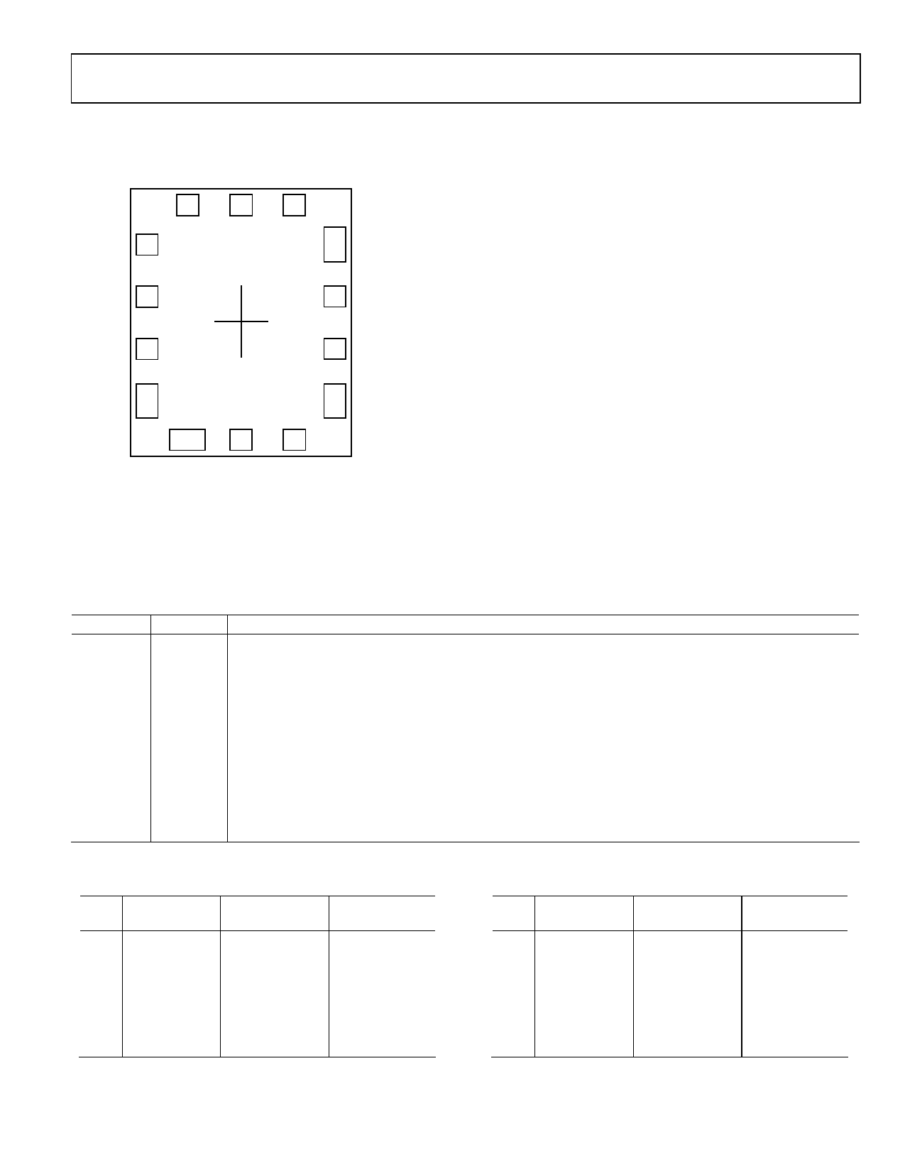
PAD LAYOUT AND FUNCTIONAL DESCRIPTIONS
PAD LAYOUT
1
VCC
14 OFFSET
2
VCC
3
VCC
GND 4
13 IN
12 TEST
OUT 5
0,0'
OUTB 6
11 GND
GND
10
CLF
9
GND 7
POWMON
8
03194-0-002
Figure 2. ADN2820 Pad Layout
DIE INFORMATION
Die Size
0.875 mm × 1.060 mm
Die Thickness
12 mils = 0.3 mm
Passivation Openings
0.08 mm × 0.08 mm
0.12 mm × 0.08 mm
0.08 mm × 0.12 mm
Passivation Composition
5000 Å Si3N4 (Top)
+5000 Å SiO2 (Bottom)
Pad Composition
Al/1% Cu
Backside Contact
P-Type Handle (Oxide Isolated from Active Circuitry)
ADN2820
PAD DESCRIPTIONS
Table 3. Pad Descriptions
Pin No.
Pad
Function
1–3
VCC
Positive Supply. Bypass to GND with a 100 pF or greater single-layer capacitor.
4, 7, 10, 11 GND
Ground.
5
OUT
Positive Output. Drives 50 Ω termination (ac or dc termination).
6
OUTB
Negative Output. Drives 50 Ω termination (ac or dc termination).
8
POWMON Input Average Power Monitor. Analog signal proportional to average optical input power. Leave open if
unused.
9
CLF
Low Frequency Cutoff Setpoint. Connect with a 0.1 μF capacitor to GND for 20 kHz.
12
TEST
Test Pad. Leave Floating.
13
IN
Current Input. Bond directly to reverse biased PIN or APD anode. Filter PIN or APD anode with 100 pF × 100 Ω
or greater.
14
OFFSET
Output Offset Adjust Input. Leave open if not being used and the input slice threshold will automatically be set
to the eye center.
PAD COORDINATES
Table 4. Pad Coordinates
Pin
No. PAD
X (mm)
1
VCC
–0.20
2
VCC
0.00
3
VCC
0.20
4
GND
0.35
5
OUT
0.35
6
OUTB
0.35
7
GND
0.35
Y (mm)
0.45
0.45
0.45
0.30
0.10
–0.10
–0.30
Pin
No. PAD
8
POWMON
9
CLF
10 GND
11 GND
12 TEST
13 IN
14 OFFSET
X (mm)
0.20
0.00
–0.20
–0.35
–0.35
–0.35
–0.35
Y (mm)
–0.45
–0.45
–0.45
–0.30
–0.10
0.10
0.30
Rev. 0 | Page 5 of 12
Share Link: 