ADN2890(Rev0) データシートの表示(PDF) - Analog Devices
部品番号
コンポーネント説明
メーカー
ADN2890 Datasheet PDF : 12 Pages
| |||
ADN2890
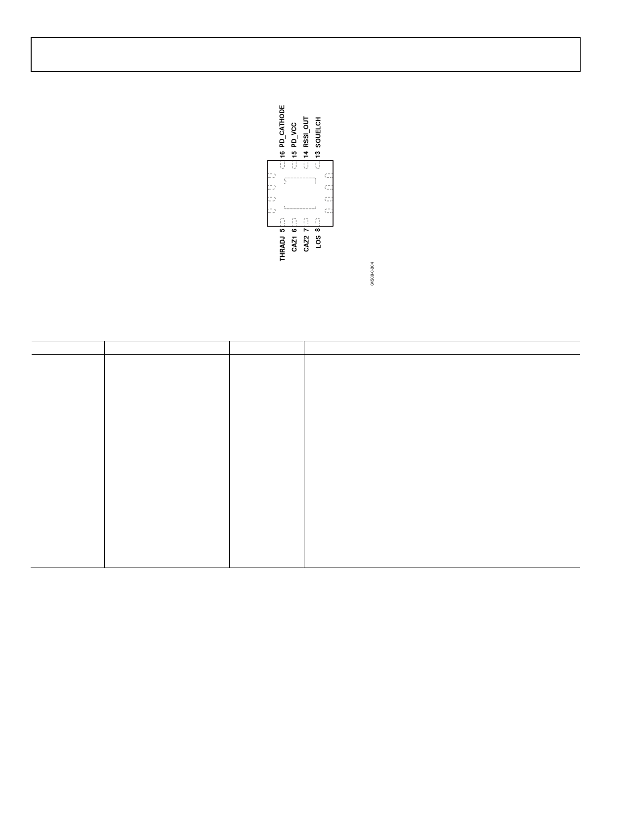
PIN CONFIGURATION AND FUNCTION DESCRIPTIONS
16 15 14 13
AVCC 1
12 DRVCC
PIN 2 ADN2890 11 OUTP
NIN 3 (NToOt TPoVSIEcWale)10 OUTN
AVEE 4
9 DRVEE
5678
Figure 2. Pin Configuration
Note: There is an exposed pad on the bottom of the package that must be connected to the GND plane with filled vias.
Table 4. Pin Function Descriptions
Pin No.
Mnemonic
1
AVCC
2
PIN
3
NIN
4
AVEE
5
THRADJ
6
CAZ1
7
CAZ2
8
LOS
9
DRVEE
10
OUTN
11
OUTP
12
DRVCC
13
SQUELCH
14
RSSI_OUT
15
PD_VCC
16
PD_CATHODE
Exposed Pad Pad
I/O
Power
Input
Input
Power
Input
Output
Power
Output
Output
Power
Input
Output
Power
Output
Power
Description
Analog Power
Differential Data Input
Differential Data Input
Analog Ground
LOS Threshold Adjust Resistor
Offset Correction Loop Capacitor
Offset Correction Loop Capacitor
LOS Detector Output
Output Buffer Ground
Differential Data Output
Differential Data Output
Output Buffer Power
Disable Outputs
Average Current Output
Power Input for RSSI Measurement
Photodiode Bias Voltage
Connect to Ground
Rev. 0 | Page 6 of 12
Share Link: 