ADP1173 データシートの表示(PDF) - Analog Devices
部品番号
コンポーネント説明
メーカー
ADP1173 Datasheet PDF : 16 Pages
| |||
ADP1173
until its FB pin is 1.245 V above its GND pin, so the output
voltage is determined by the formula:
–V OUT
= 1.245
V
×
1+
R1
R2
+VIN
+
C2
R3
1
2
3
ILIM VIN SW1
FB 8
ADP1173
SW2 4
GND
5
L1
+
C1
D1
1N5818
R1
R2
–VOUT
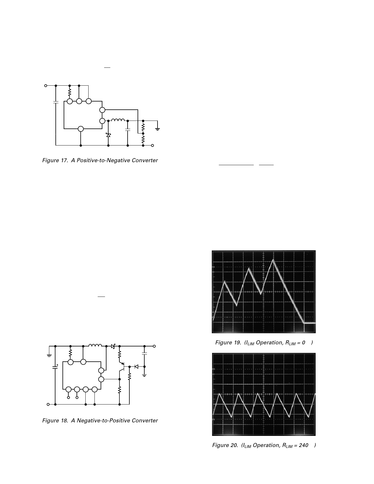
Figure 17. A Positive-to-Negative Converter
The design criteria for the step-down application also apply to
the positive-to-negative converter. The output voltage should be
limited to |6.2 V|, unless a diode is inserted in series with the
SW2 Pin (see Figure 16). Also, D1 must again be a Schottky
diode to prevent excessive power dissipation in the ADP1173.
NEGATIVE-TO-POSITIVE CONVERSION
The circuit of Figure 18 converts a negative input voltage to a
positive output voltage. Operation of this circuit configuration is
similar to the step-up topology of Figure 14, except that the current
through feedback resistor R1 is level-shifted below ground by a
PNP transistor. The voltage across R1 is (VOUT–VBEQ1). How-
ever, diode D2 level-shifts the base of Q1 about 0.6 V below
ground, thereby cancelling the VBE of Q1. The addition of D2
also reduces the circuit’s output voltage sensitivity to tempera-
ture, which otherwise would be dominated by the –2 mV/°C VBE
contribution of Q1. The output voltage for this circuit is deter-
mined by the formula:
V OUT
= 1.245
V
×
R1
R2
Unlike the positive step-up converter, the negative-to-positive
converter’s output voltage can be either higher or lower than the
input voltage.
1N5818
L1
D1
RLIM
R1
1
2
C2
ILIM
VIN
SW1 3
Q1
2N3906
ADP1173
FB 8
AO SET GND SW2
6754
R2
POSITIVE
+
OUTPUT
CL
1N4148
D2
10kΩ
NEGATIVE
INPUT
NC NC
LIMITING THE SWITCH CURRENT
The ADP1173’s RLIM pin permits the switch current to be lim-
ited with a single resistor. This current limiting action occurs on
a pulse by pulse basis. This feature allows the input voltage to
vary over a wide range, without saturating the inductor or ex-
ceeding the maximum switch rating. For example, a particular
design may require peak switch current of 800 mA with a 2.0 V
input. If VIN rises to 4 V, however, the switch current will exceed
1.6 A. The ADP1173 limits switch current to 1.5 A and thereby
protects the switch, but increases the output ripple. Selecting
the proper resistor will limit the switch current to 800 mA, even
if VIN increases. The relationship between RLIM and maximum
switch current is shown in Figures 4 and 5.
The ILIM feature is also valuable for controlling inductor current
when the ADP1173 goes into continuous-conduction mode. This
occurs in the step-up mode when the following condition is met:
VOUT +V DIODE < 1
V IN –V SW 1– DC
where DC is the ADP1173’s duty cycle. When this relationship
exists, the inductor current does not go all the way to zero dur-
ing the time the switch is OFF. When the switch turns on for
the next cycle, the inductor current begins to ramp up from the
residual level. If the switch ON time remains constant, the in-
ductor current will increase to a high level (see Figure 19). This
increases output ripple, and can require a larger inductor and
capacitor. By controlling switch current with the ILIM resistor,
output ripple current can be maintained at the design values.
Figure 20 illustrates the action of the ILIM circuit.
Figure 19. (ILIM Operation, RLIM = 0 Ω)
Figure 18. A Negative-to-Positive Converter
–10–
Figure 20. (ILIM Operation, RLIM = 240 Ω)
REV. 0
Share Link: 