ADP2102-1.2-EVALZ(RevC) データシートの表示(PDF) - Analog Devices
部品番号
コンポーネント説明
メーカー
ADP2102-1.2-EVALZ
(Rev.:RevC)
(Rev.:RevC)
Analog Devices

ADP2102-1.2-EVALZ Datasheet PDF : 24 Pages
| |||
Data Sheet
Low Duty Cycle, 600 mA, 3 MHz, Synchronous
Step-Down DC-to-DC Converter
ADP2102
FEATURES
Input voltage range: 2.7 V to 5.5 V
600 mA maximum load current
95% efficiency
Low duty cycle operation
Only 3 tiny external ceramic components
3 MHz typical operating frequency
Fixed output voltage of 1.2 V or 1.375 V
Adjustable output voltage up to 3.3 V
0.01 µA shutdown supply current
Automatic power save mode
Internal synchronous rectifier
Internal soft start
Internal compensation
Enable/shutdown logic input
Undervoltage lockout
Current limit protection
Thermal shutdown
Small 8-lead, 3 mm × 3 mm LFCSP
APPLICATIONS
USB powered devices
WLAN and gateways
Point of loads
Processor core power from 5 V
Digital cameras
PDAs and palmtop computers
Portable media players, GPS
GENERAL DESCRIPTION
The ADP2102 is a synchronous step-down dc-to-dc converter
that converts a 2.7 V to 5.5 V unregulated input voltage to a lower
regulated output voltage with up to 95% efficiency and 1%
accuracy. The low duty cycle capability of the ADP2102 is ideal for
USB applications or 5 V systems that power up submicron subvolt
processor cores. Its 3 MHz typical operating frequency and excel-
lent transient response allow the use of small, low cost 1 µH
inductors and 2.2 µF ceramic capacitors. At medium-to-high
load currents, it uses a current mode, pseudofixed frequency pulse-
width modulation to extend battery life. To ensure the longest
battery life in portable applications, the ADP2102 has a power save
mode (PSM) that reduces the switching frequency under light
load conditions to significantly reduce quiescent current.
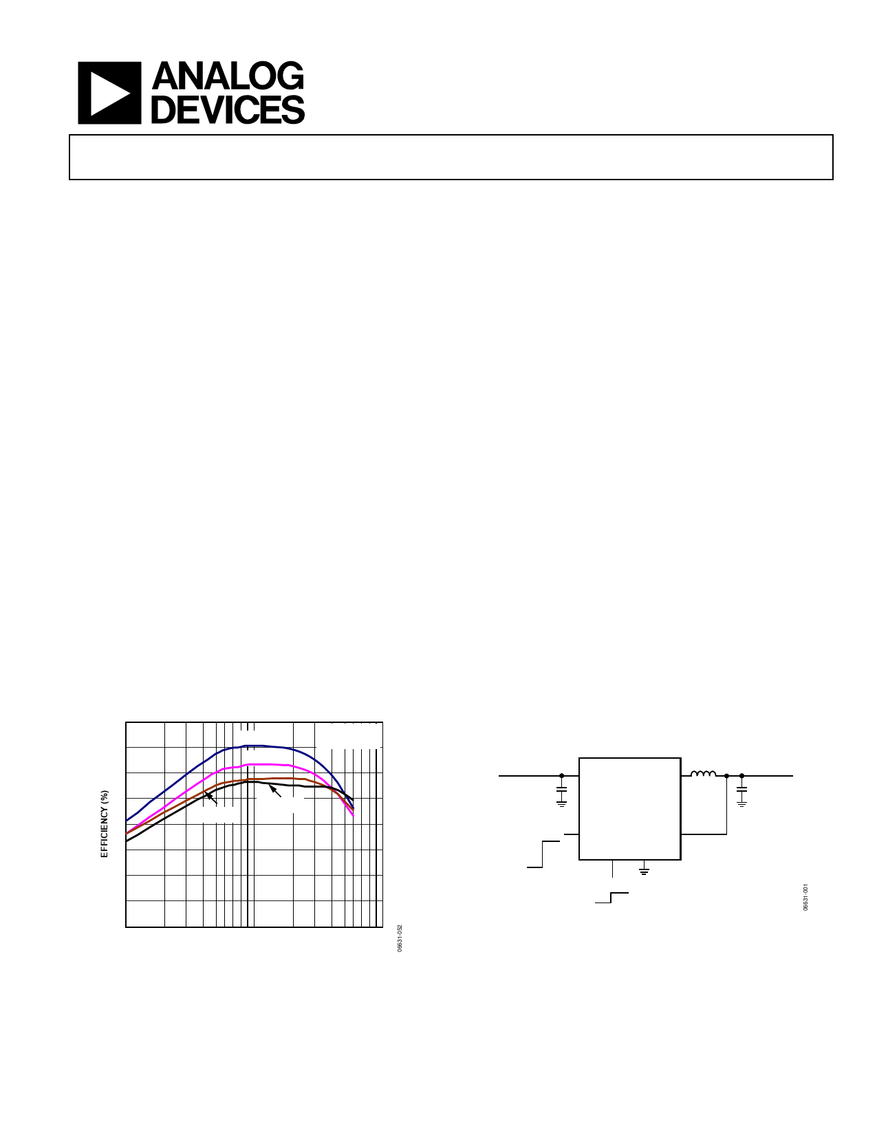
TYPICAL APPLICATION CIRCUIT
INPUT VOLTAGE
2.7V TO 5.5V
CIN
2.2µF
FORCED
CCM
DCM/
CCM
VIN
LX
ADP2102
MODE
EN
FB/OUT
GND
ON
OFF
OUTPUT VOLTAGE
L 1.2V OR 1.375V
1µH
COUT
2.2µF
Figure 1.
The ADP2102 is available in both fixed and adjustable output
voltage options with a 600 mA maximum output current. The fixed
output voltage options are 1.2 V and 1.375 V. The adjustable output
voltage options are available from 1.5 V to 3.3 V. The ADP2102
requires only three external components and consumes 0.01 µA
in shutdown mode.
The ADP2102 is available in an 8-lead LFCSP and is specified
for the −40°C to +85°C temperature range.
100
95
VIN = 2.7V
VOUT = 1.375V
TA = 25°C
VIN = 3V
90
85
VIN = 4.2V
VIN = 3.6V
80
75
70
65
60
10
100
LOAD CURRENT (mA)
1000
Figure 2. Efficiency vs. Load Current at VOUT = 1.375 V
Rev. C
Document Feedback
Information furnished by Analog Devices is believed to be accurate and reliable. However, no
responsibility is assumed by Analog Devices for its use, nor for any infringements of patents or other
rights of third parties that may result from its use. Specifications subject to change without notice. No
license is granted by implication or otherwise under any patent or patent rights of Analog Devices.
Trademarks and registered trademarks are the property of their respective owners.
One Technology Way, P.O. Box 9106, Norwood, MA 02062-9106, U.S.A.
Tel: 781.329.4700 ©2007–2016 Analog Devices, Inc. All rights reserved.
Technical Support
www.analog.com
Share Link: