ADP2102-4-EVALZ(RevC) データシートの表示(PDF) - Analog Devices
部品番号
コンポーネント説明
メーカー
ADP2102-4-EVALZ
(Rev.:RevC)
(Rev.:RevC)
ADP2102-4-EVALZ Datasheet PDF : 24 Pages
| |||

ADP2102
ABSOLUTE MAXIMUM RATINGS
Table 2.
Parameter
AVIN, EN, MODE, FB/OUT to AGND
LX to PGND
PVIN to PGND
PGND to AGND
AVIN to PVIN
Operating Ambient Temperature Range
Junction Temperature Range
Storage Temperature Range
Soldering Conditions
Rating
−0.3 V to +6 V
−0.3 V to (VIN + 0.3 V)
−0.3 V to +6 V
−0.3 V to +0.3 V
−0.3 V to +0.3 V
−40°C to +85°C1
−40°C to +125°C
−65°C to +150°C
JEDEC J-STD-020
1 The ADP2102 can be damaged when junction temperature limits are exceeded.
Monitoring ambient temperature does not guarantee that TJ is within the
specified temperature limits. In applications where high power dissipation
and poor thermal resistance are present, the maximum ambient temperature
may have to be derated. In applications with moderate power dissipation
and low PCB thermal resistance, the maximum ambient temperature can
exceed the maximum limit as long as the junction temperature is within
specification limits. The junction temperature (TJ) of the device is dependent
on the ambient temperature (TA), the power dissipation of the device (PD),
and the junction-to-ambient thermal resistance of the package (θJA). Maximum
junction temperature (TJ) is calculated from the ambient temperature (TA)
and power dissipation (PD) using the formula TJ = TA + (θJA × PD). Unless
otherwise specified, all other voltages are referenced to AGND.
Stresses at or above those listed under Absolute Maximum
Ratings may cause permanent damage to the product. This is a
stress rating only; functional operation of the product at these
or any other conditions above those indicated in the operational
section of this specification is not implied. Operation beyond
the maximum operating conditions for extended periods may
affect product reliability.
Data Sheet
THERMAL RESISTANCE
Junction-to-ambient thermal resistance (θJA) of the package is
based on modeling and calculation using a 4-layer board. The
junction-to-ambient thermal resistance is highly dependent on
the application and board layout. In applications where high
maximum power dissipation exists, attention to thermal board
design is required. The value of θJA may vary, depending on PCB
material, layout, and environmental conditions. Specified value
of θJA is based on a 4-layer, 4 in × 3 in, 2 1/2 oz copper board,
as per JEDEC standards. For more information, see the AN-772
Application Note, A Design and Manufacturing Guide for the
Lead Frame Chip Scale Package (LFCSP).
Table 3. Thermal Resistance
Package Type
θJA
Unit
8-Lead LFCSP
54
°C/W
Maximum Power Dissipation
0.74
W
BOUNDARY CONDITION
Natural convection, 4-layer board, exposed pad soldered to PCB.
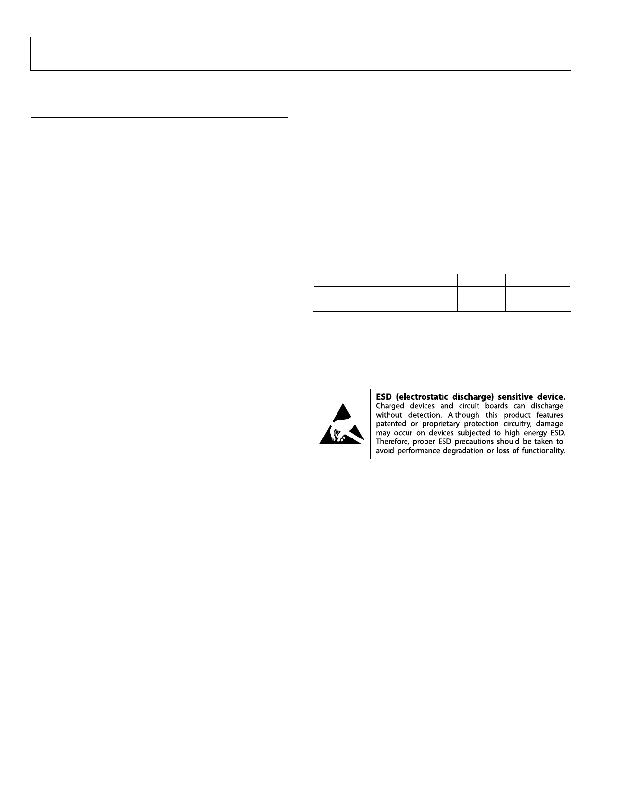
ESD CAUTION
Rev. C | Page 4 of 24