ADP2102-EVAL データシートの表示(PDF) - Analog Devices
部品番号
コンポーネント説明
メーカー
ADP2102-EVAL Datasheet PDF : 7 Pages
| |||
Preliminary Technical Data
FEATURES
95% peak efficiency
Optimized for low output voltages
Optimized for extremely small ceramic inductors
Up to 600mA, load current
2.7 V to 5.5 V input voltage range
Operates with a Single Li-Ion battery
Fixed Output Voltage from 0.8V to 1.875V
Adjustable Output Voltage from 0.8V to 1.875V
Low 60μA quiescent current
Internal Synchronous rectifier
3 MHz Operating Frequency
0.1μA Shutdown Supply Current
Small 8-Lead 3 x3 LFCSP Package
Enable /shutdown logic input
Under Voltage Lockout
Internal Soft Start
Internal Compensation
APPLICATIONS
Wireless Handsets
Portable Media Players
PDA’s and Palmtop Computers
Digital Cameras
Smart Phones
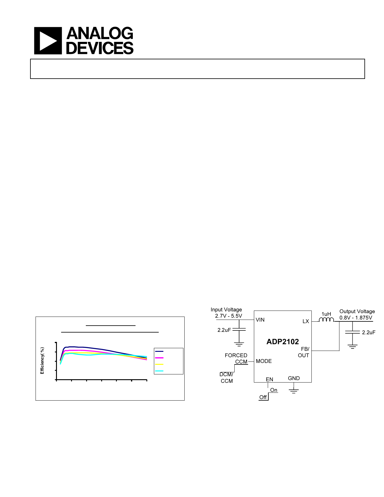
TYPICAL PERFORMANCE CHARACTERITICS
ADP2102_Efficiency
Vout= 1.375V L =2.2uH Cin= Cout = 10uF
100
90
80
70
60
0
100 200 300 400 500 600
Load Current ( mA)
Vin= 2.7V
Vin=3.0V
Vin=3.6V
Vin=4.2V
Figure 1.
600mA 3MHz Synchronous
Step-Down DC-DC Converter
ADP2102
GENERAL DESCRIPTION
The ADP2102 is a low quiescent current step-down DC-DC
converter optimized to regulate low output voltages in a
compact 3mmx3mm LFCSP package. At high load currents, the
ADP2102 uses a current mode, constant on time, pseudo fixed
frequency, valley current control scheme for excellent stability
and transient response with very few, small external
components. To ensure the longest battery life in portable
applications, the ADP2102 has a power saving mode that
reduces the switching frequency under light load conditions to
significantly reduce the quiescent current.
The ADP2102 runs from input voltages from 2.7V to 5.5V
allowing single Li+/Li- polymer cell, multiple Alkaline/Ni-MH
cells and other standard power sources. ADP2102 output
voltage is adjustable from 0.8V to 1.875V, while the suffix part
numbers ADP2102-XX indicate pre-set voltage ranges of 1.875,
1.8, 1.5, 1.375, 1.25, 1.2, 1.0 & 0.8V. All versions include an
internal power switch and a synchronous rectifier for high
efficiency while internal compensation guarantees minimal
number of external components. During logic-controlled
shutdown, the input is disconnected from the output and it
draws less than 0.1μA from the input source. Other key features
include under voltage lockout to prevent deep battery discharge
and soft start to prevent input current overshoot at startup.
TYPICAL APPLICATION CIRCUIT
Figure 2.
Rev. PrA
Information furnished by Analog Devices is believed to be accurate and reliable. However, no
responsibility is assumed by Analog Devices for its use, nor for any infringements of patents or other
rights of third parties that may result from its use. Specifications subject to change without notice. No
license is granted by implication or otherwise under any patent or patent rights of Analog Devices.
Trademarks and registered trademarks are the property of their respective owners.
One Technology Way, P.O. Box 9106, Norwood, MA 02062-9106, U.S.A.
Tel: 781.329.4700
www.analog.com
Fax: 781.461.3113
©2007 Analog Devices, Inc. All rights reserved.
Share Link: 