ADP3026 データシートの表示(PDF) - Analog Devices
部品番号
コンポーネント説明
メーカー
ADP3026 Datasheet PDF : 20 Pages
| |||
ADP3026
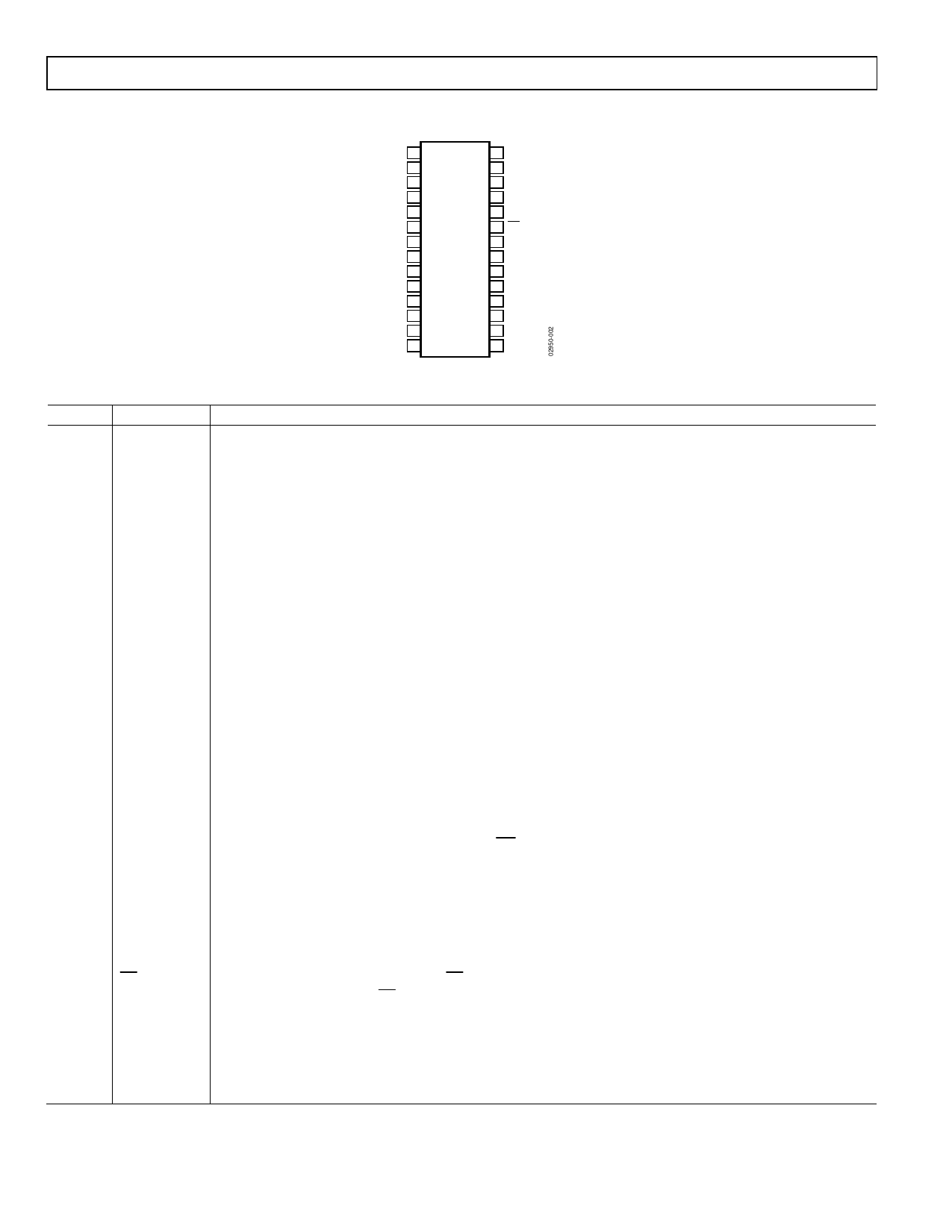
PIN CONFIGURATION AND FUNCTION DESCRIPTIONS
CS5 1
28 BST5
FB5 2
27 DRVH5
EAN5 3
26 SW5
EAO5 4 ADP3026 25 DRVL5
SS5 5
24 PGND
TOP VIEW
CLSET5 6 (Not to Scale) 23 SD
REF 7
22 INTVCC
AGND 8
21 VIN
CLSET3 9
20 DRVL3
SS3 10
19 SW3
EAO3 11
18 DRVH3
EAN3 12
17 BST3
FB3 13
16 CPOR
CS3 14
15 PWRGD
Figure 2. 28-Lead TSSOP Pin Configuration
Table 3. Pin Function Descriptions
Pin No. Mnemonic Function
1
CS5
Current Sense Input for the Top N-Channel MOSFET of the 5 V Buck Converter. Connect to the drain of the top
N-channel MOSFET.
2
FB5
Feedback Input for the 5 V Buck Converter. Connect to the output sense point in fixed output mode.
3
EAN5
Inverting Input of the Error Amplifier of the 5 V Buck Converter. Use for external loop compensation.
4
EAO5
Error Amplifier Output for the 5 V Buck Converter.
5
SS5
Soft Start for the 5 V Buck Converter. Also used as an on/off pin.
6
CLSET5
Current Limit Setting. A resistor can be connected from AGND to CLSET5. A minimum current limit is obtained
by leaving it unconnected. A maximum current limit is obtained by connecting it to AGND.
7
REF
800 mV Band Gap Reference. Bypass it with a capacitor (22 nF typical) to AGND. REF cannot be used directly
with an external load.
8
AGND
Analog Signal Ground.
9
CLSET3
Current Limit Setting. A resistor can be connected from AGND to CLSET3. A minimum current limit is obtained
by leaving it unconnected. A max current limit is obtained by connecting it to AGND.
10
SS3
Soft Start for the 3.3 V Buck Converter. Also used as an on/off pin.
11
EAO3
Error Amplifier Output for the 3.3 V Buck Converter.
12
EAN3
Error Amplifier Inverting Input of the 3.3 V Buck Converter. Use for external loop compensation.
13
FB3
Feedback Input for the 3.3 V Buck Converter. Connect to output sense point.
14
CS3
Current Sense Input for the Top N-Channel MOSFET of the 3.3 V Buck Converter. It should be connected to the
drain of the N-channel MOSFET.
15
PWRGD
Power Good Output. PWRGD goes low with no delay whenever the 5 V output drops 7% below its nominal
value. When the 5 V output is within −3% of its nominal value, PWRGD will be released after a time delay
determined by the timing capacitor on the CPOR pin.
16
CPOR
Connect a capacitor between CPOR and AGND to set the delay time for the PWRGD pin. A 1 µA pull-up current
is used to charge the capacitor. A manual reset (MR) function can also be implemented by grounding this pin.
17
BST3
Boost Capacitor Connection for High-Side Gate Driver of the 3.3 V Buck Converter.
18
DRVH3
High-Side Gate Driver for the 3.3 V Buck Converter.
19
SW3
Switching Node (Inductor) Connection of the 3.3 V Buck Converter.
20
DRVL3
Low-Side Gate Driver of the 3.3 V Buck Converter.
21
VIN
Main Supply Input (5.5 V to 25 V).
22
INTVCC
Linear Regulator Bypass for the internal 5 V LDO. Bypass this pin with a 4.7 µF capacitor to AGND.
23
SD
Shutdown Control Input, Active Low. If SD = 0 V, the chip is in shutdown with very low quiescent current. For
automatic startup, connect SD to VIN directly.
24
PGND
Power Ground.
25
DRVL5
Low-Side Driver for the 5 V Buck Converter.
26
SW5
Switching Node (Inductor) Connection for the 5 V Buck Converter.
27
DRVH5
High-Side Gate Driver for the 5 V Buck Converter.
28
BST5
Boost Capacitor Connection for the High-Side Gate Driver of the 5 V Buck Converter.
Rev. 0 | Page 6 of 20
Share Link: 